Light emitting-diode chip and a method for producing same

a technology of light-emitting diodes and chips, which is applied in the direction of basic electric elements, electrical apparatus, and semiconductor devices, can solve the problems of high technical expenditure, insufficient maximum attainable electrical conductivity of p-doped layers, especially of p-doped gan or algan layers, and insufficient economic justification, etc., to achieve the effect of increasing luminous efficiency

Inactive Publication Date: 2008-01-15
OSRAM OLED
View PDF143 Cites 60 Cited by
  • Summary
  • Abstract
  • Description
  • Claims
  • Application Information

AI Technical Summary

Benefits of technology

[0008]The object of the invention is, first, to develop an LED chip of the kind described at the beginning hereof that offers improved current spread and whose additional production expenditure is kept to a minimum. A method of fabricating an LED component comprising such a chip is also to be provided.
[0010]The substrate advantageously serves here as a window layer that improves the decoupling of the radiation generated inside the chip. To optimize its thickness, the substrate is advantageously thinned, for example by grinding and / or etching, after the growth of the epitaxial layer sequence.
[0013]The particular advantage of such a so-called thin-film LED chip lies in the reduced, ideally nonexistent, absorption of radiation in the chip and the improved decoupling of radiation from the chip, especially due to the smaller number of interfaces with jumps in the refractive index.
[0014]Both of the LED chips according to the invention have the particular advantage that the lost-heat-producing region (especially the p-doped layer and the p-n junction) of the chip can be situated very close to a heat sink; the epitaxial layer sequence can be thermally coupled to a heat sink practically directly. This enables the chip to be cooled very effectively, thereby increasing the stability of the emitted radiation. The efficiency of the chip is also increased.
[0016]In the LED chip of the invention, the p-contact layer comprises, deposited on the p-side, a transparent first layer, and deposited thereon, a second, reflective layer. The contact layer can thus be optimized in a simple manner with regard to both its electrical and its reflective properties.
[0019]In a further preferred embodiment, the entire bare surface of, or a subarea of, the semiconductor body formed by the layer sequence is roughened. This roughening disrupts the total reflection at the decoupling surface, thereby advantageously further increasing the degree of optical decoupling.

Problems solved by technology

A fundamental problem in the fabrication of GaN-based light-emitting diode (LED) chips is that the maximum attainable electrical conductivity of p-doped layers, especially of p-doped GaN or AlGaN layers, is not sufficient, in conventional LED chips made of other material systems, to effect the spread of current over the entire lateral cross section of the chip, since the front contacts normally used in such chips are made to cover only a fraction of the front of the chip in order to bring about the highest possible decoupling of radiation.
Growing the p-type layer on an electrically conductive substrate, which would make it possible to impress a current over the entire lateral cross section of the p-type layer, does not furnish economically justifiable results.
The reasons for this are that fabricating electrically conductive lattice-matched substrates (e.g. GaN substrates) for the growth of GaN-based layers involves high technical expenditure, and growing p-doped GaN-based layers on non-lattice-matched substrates suitable for undoped and n-doped GaN compounds does not yield adequate crystal quality for an LED.
However, the first-cited proposal has the disadvantage that a substantial portion of the radiation is absorbed in the contact layer.

Method used


Image

  • Light emitting-diode chip and a method for producing same
  • Light emitting-diode chip and a method for producing same
  • Light emitting-diode chip and a method for producing same

Examples


Embodiment Construction

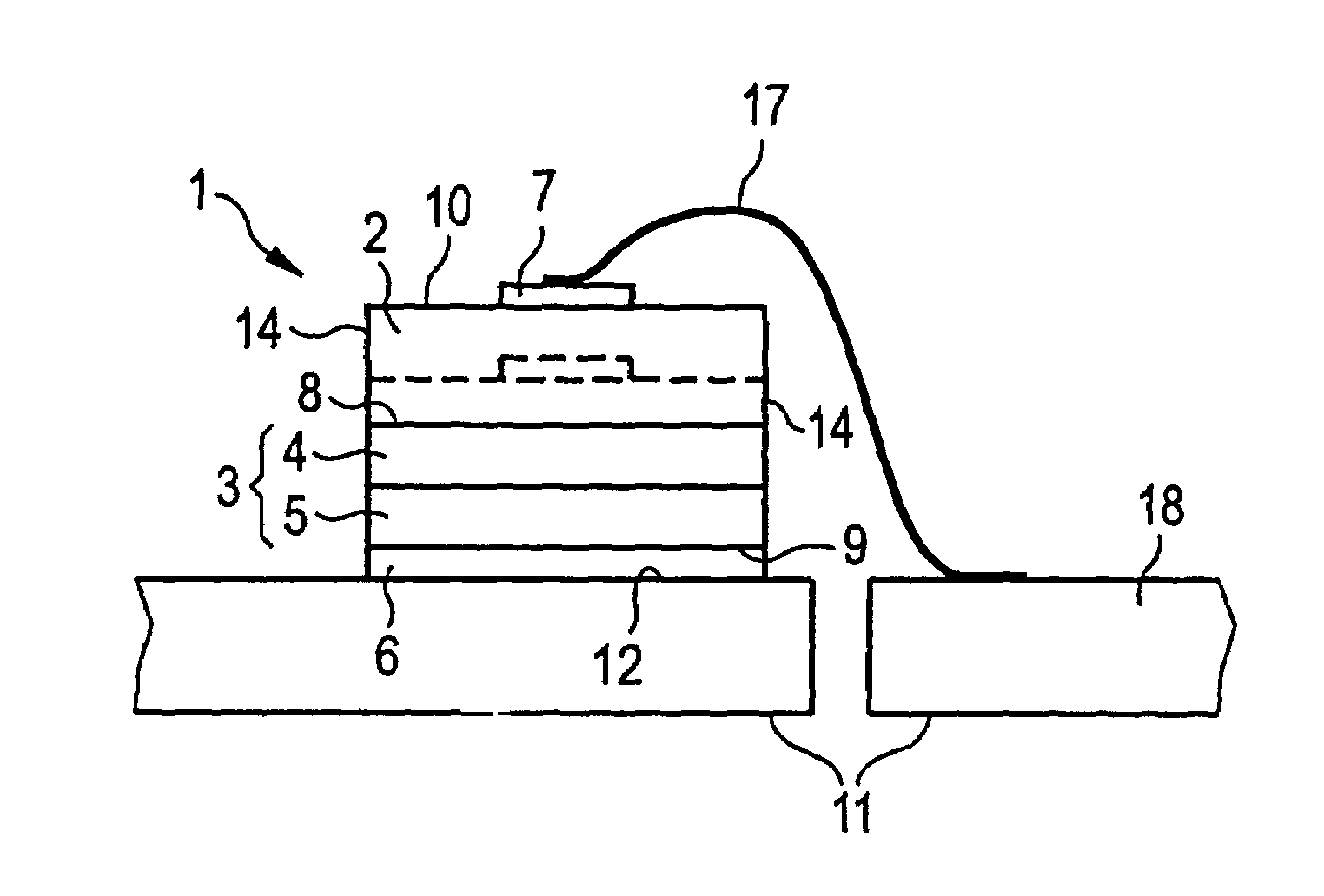
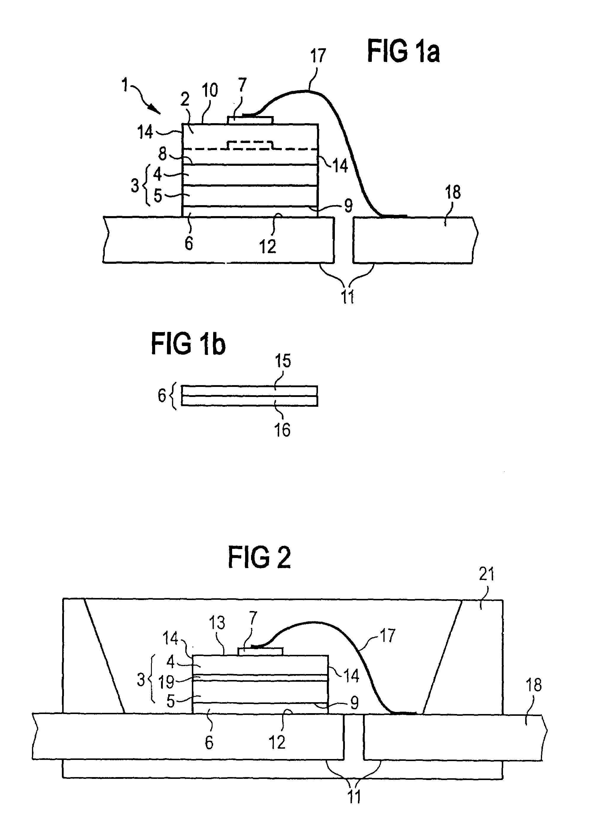
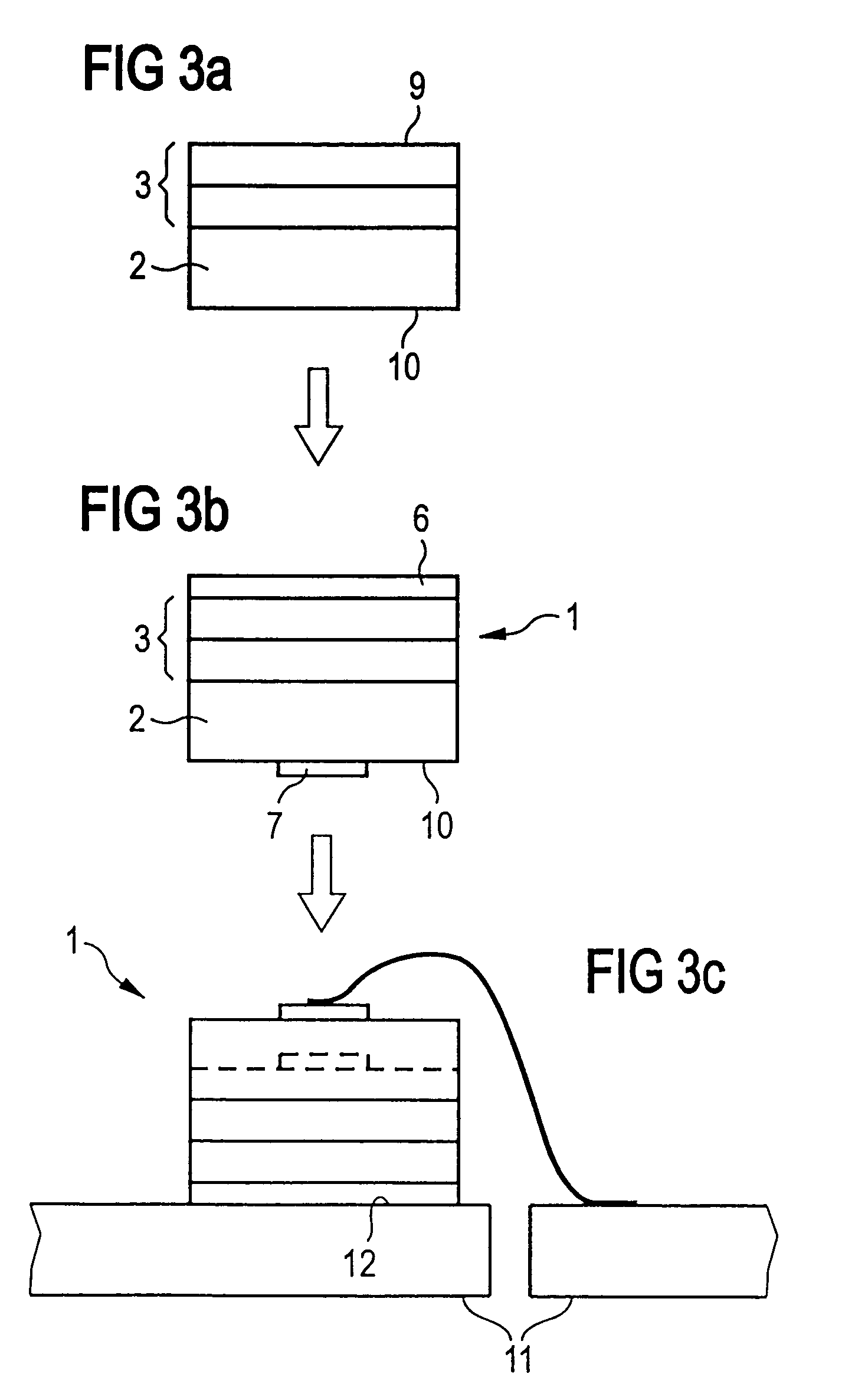
[0030]In the LED chip 1 of FIG. 1a, deposited on an SiC substrate 2 is a radiation-emitting epitaxial layer sequence 3 on an n-type side 8 of the substrate 2. This comprises, for example, an n-type doped GaN or AlGaN epitaxial layer 4 and a p-type doped GaN or AlGaN epitaxial layer 5. There can also be provided, for example, a GaN-based epitaxial layer sequence 3 having a double heterostructure, a single quantum well (SQW) structure or a multi-quantum well (MQW) structure comprising one or more undoped layers 19, for example of InGaN or InGaAlN.

[0031]The SiC substrate 2 is electrically conductive and is opaque to the radiation emitted by epitaxial layer sequence 3.

[0032]The p-side 9 of epitaxial layer sequence 3 facing away from the SiC substrate 2 comprises, deposited over substantially its full area, a reflective, bondable p-contact layer 6. This is composed, for example, substantially of Ag, a PtAg alloy and / or a PdAg alloy.

[0033]However, as illustrated schematically in FIG. 1b, ...


PUM


Abstract

An LED chip comprising an electrically conductive and radioparent substrate, in which the epitaxial layer sequence (3) is provided on substantially the full area of its p-side (9) with a reflective, bondable p-contact layer (6). The substrate (2) is provided on its main surface (10) facing away from the epitaxial layer sequence (3) with a contact metallization (7) that covers only a portion of said main surface (10), and the decoupling of light from the chip (1) takes place via a bare region of the main surface (10) of the substrate (2) and via the chip sides (14). A further LED chip has epitaxial layers only. The p-type epitaxial layer (5) is provided on substantially the full area of the main surface (9) facing away from the n-conductive epitaxial layer (4) with a reflective, bondable p-contact layer (6), and the n-conductive epitaxial layer (4) is provided on its main surface facing away from the p-conductive epitaxial layer (5) with an n-contact layer (7) that covers only a portion of said main surface (8). The decoupling of light from the chip (1) takes place via the bare region of the main surface (8) of the n-conductive epitaxial layer (4) and via the chip sides (14).

Description

CROSS REFERENCE TO RELATED APPLICATIONS[0001]This application is the U.S. National Phase application of WIPO Application No. PCT / DE01 / 01003, filed on Mar. 16, 2001, which claims the benefit of foreign priority applications filed in Germany, Serial Nos. 10026255.4, filed on May 26, 2000, and 10020464.3, filed on Apr. 26, 2000.FIELD OF THE INVENTION[0002]The invention concerns a light-emitting diode and a method for fabricating the same.BACKGROUND OF THE INVENTION[0003]A fundamental problem in the fabrication of GaN-based light-emitting diode (LED) chips is that the maximum attainable electrical conductivity of p-doped layers, especially of p-doped GaN or AlGaN layers, is not sufficient, in conventional LED chips made of other material systems, to effect the spread of current over the entire lateral cross section of the chip, since the front contacts normally used in such chips are made to cover only a fraction of the front of the chip in order to bring about the highest possible deco...

Claims


Application Information

Patent Timeline
Patent Type & Authority Patents(United States)
IPC IPC(8): H01L33/00H01L27/15H01L33/10H01L33/14H01L33/32H01L33/40H01L33/60H01L33/62
CPCH01L33/0079H01L33/10H01L33/405H01L33/145H01L33/32H01L33/40H01L33/60H01L33/62H01L2224/32245H01L2224/48247H01L2224/48472H01L2224/73265H01L2224/48091H01L2924/00014H01L2924/00H01L2924/181H01L33/0093H01L2924/00012
Inventor BADER, STEFANHAHN, BERTHOLDHARLE, VOLKERLUGAUER, HANS-JURGENMUNDBROD-VANGEROW, MANFRED
Owner OSRAM OLED
Why Eureka
Try Eureka