Semiconductor light-emitting device using phosphors for performing wavelength conversion

a technology of phosphors and semiconductors, applied in the direction of discharge tubes/lamp details, discharge tubes luminescnet screens, electric discharge lamps, etc., can solve the problems of long-life reliability and environmental resistance of organic el-based displays, disadvantages of lcd-based displays, and low display speed, so as to achieve superior environmental resistance and light loss. , the effect of high display speed

Active Publication Date: 2008-01-29
SANKEN ELECTRIC CO LTD
View PDF12 Cites 226 Cited by
  • Summary
  • Abstract
  • Description
  • Claims
  • Application Information

AI Technical Summary

Benefits of technology

[0006]An object of the present invention is to solve the above problems. The present invention provides a semiconductor light-emitting device, a light-emitting display, a method for manufacturing a semiconductor light-emitting device and a method for manufacturing a light-emitting display, in which the display speed is high, long-life reliability, superior environmental resistance, a small loss of light, low energy requirements, simplified manufacturing processes, and cost reduction can be achieved.

Problems solved by technology

However, in a case where high-definition and high-reliability images or moving images are desired to be obtained, LCD-based displays are disadvantageous in that display speed is low.
Meanwhile, organic EL-based displays have problems of long-life reliability and environmental resistance.
Furthermore, LCD or organic EL-based displays are disadvantageous in that a large loss of light due to windows and color filters occurs and thus excess energy is required.
In addition, there are problems of the complexity of manufacturing processes and the difficulty of cost reduction.

Method used


Image

  • Semiconductor light-emitting device using phosphors for performing wavelength conversion
  • Semiconductor light-emitting device using phosphors for performing wavelength conversion
  • Semiconductor light-emitting device using phosphors for performing wavelength conversion

Examples


first embodiment

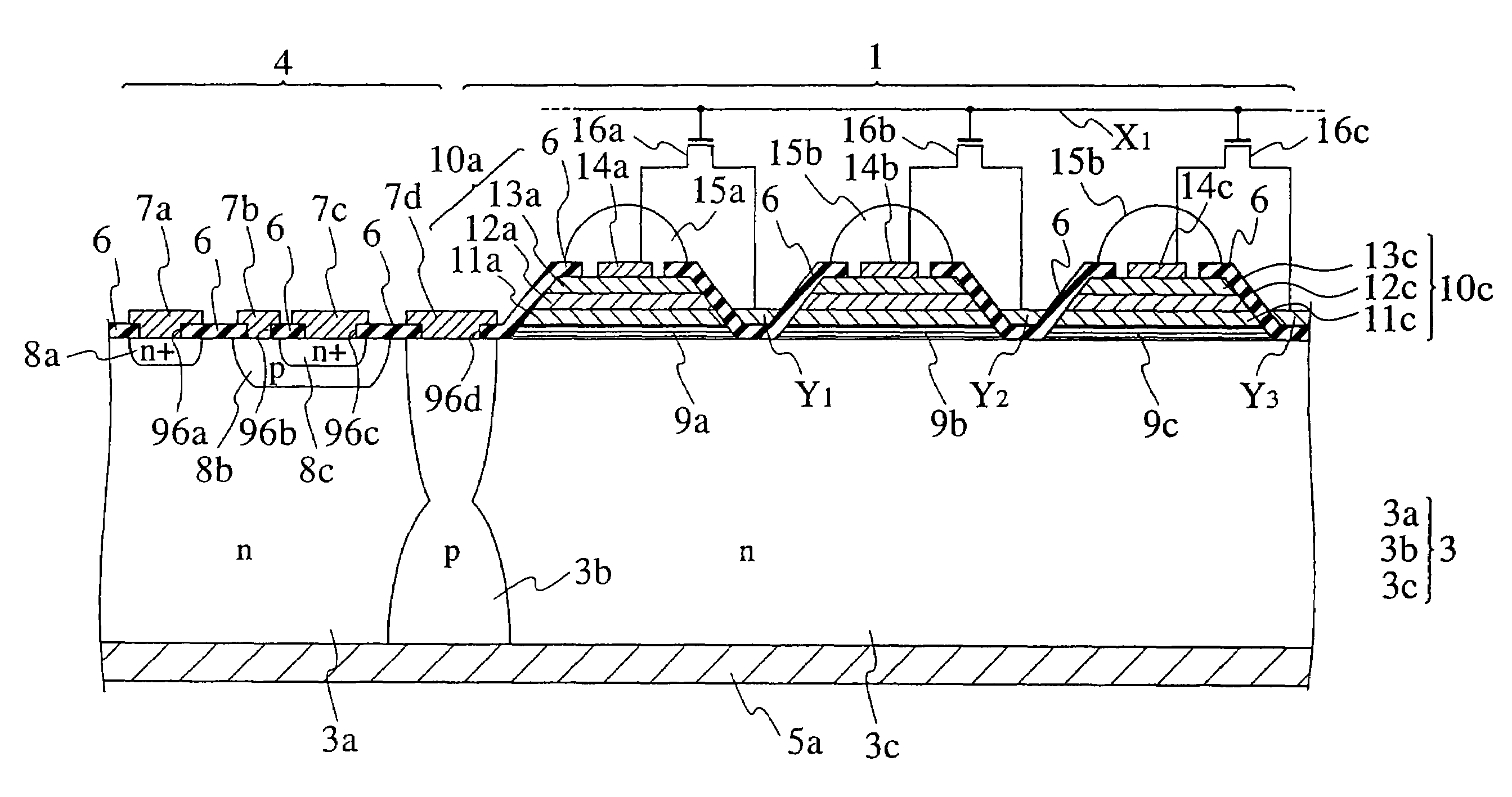
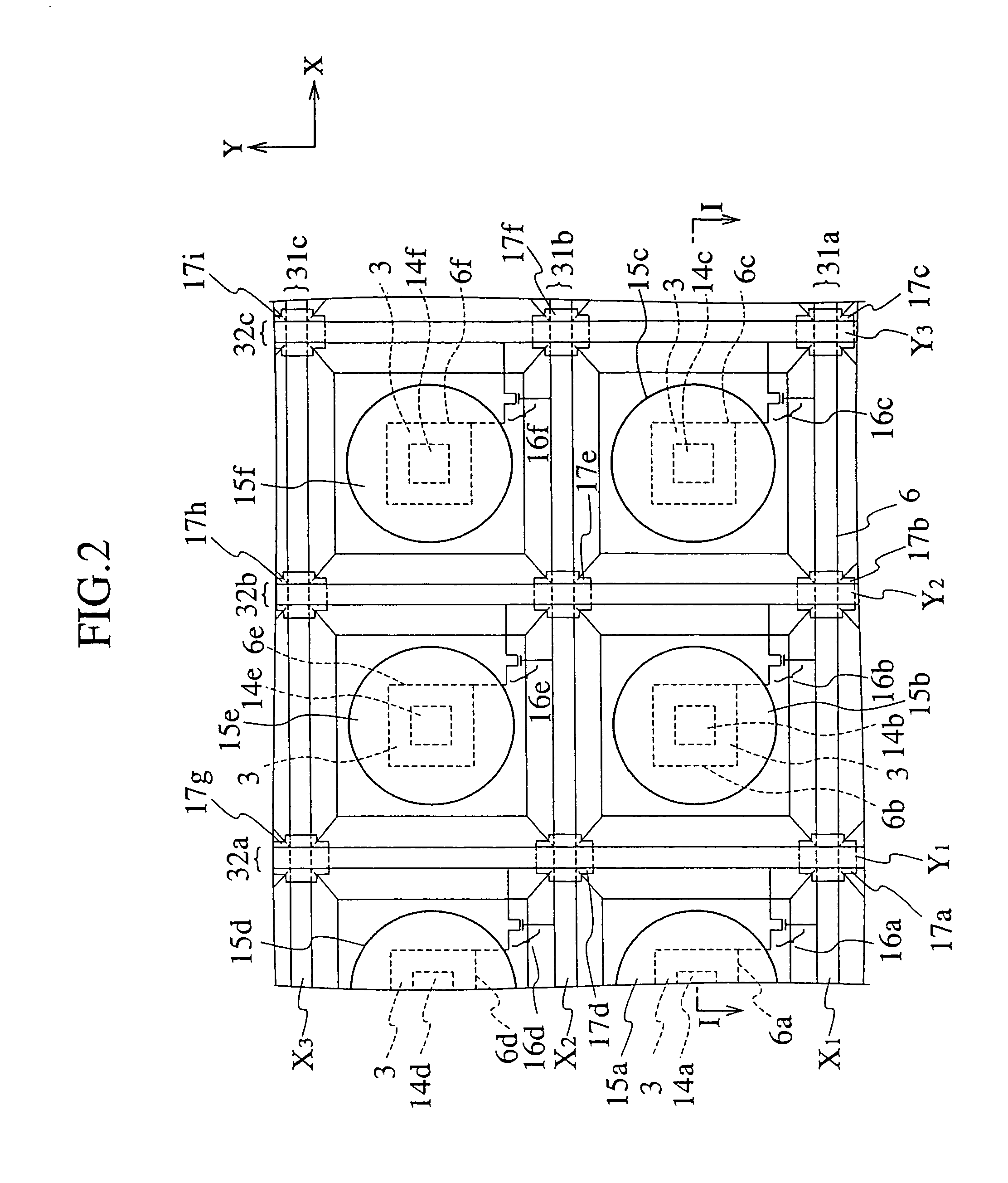
[0028]As shown in FIG. 1, a light-emitting display according to a first embodiment of the present invention includes a substrate 3, a plurality of (first to third) light-emitting-element-layers 10a, 10b and 10c formed on the substrate 3 so as to be isolated from each other, and first to third phosphors 15a, 15b and 15c which are placed on the first to third light-emitting-element-layers 10a, 10b and 10c and convert wavelengths of light from the first to third light-emitting-element-layers 10a, 10b and 10c into different wavelengths.

[0029]FIG. 1 shows a semiconductor light-emitting device including the first to third light-emitting-element-layers 10a, 10b and 10c and the first to third phosphors 15a, 15b and 15c which constitute one unit picture element (pixel). However, in the light-emitting display according to the first embodiment of the present invention, a plurality of unit picture elements (pixels) constituting an m×n matrix which constitutes the light-emitting display body, ar...

second embodiment

[0060]In a light-emitting display according to a second embodiment of the present invention, a driving circuit section 4a is monolithically integrated in the same wafer as that of a light-emitting display section 1, as shown in FIG. 7. The light-emitting display section 1 has substantially the same structure and function as that of the light-emitting display according to the first embodiment of the present invention shown in FIG. 1. Moreover, the driving circuit section 4a has substantially the same structure and function as that of the driving circuit 4 shown in FIG. 3.

[0061]As shown in FIG. 7, the light-emitting display according to the second embodiment of the present invention includes a substrate 3, a plurality of (first to third) light-emitting-element-layers 10a, 10b and 10c made of semiconductor materials which are formed on the substrate 3 so as to be isolated from each other and which have wider band gaps than the substrate 3, and first to third phosphors 15a, 15b and 15c ...

third embodiment

[0078]As shown in FIG. 10, the light-emitting display according to the third embodiment of the present invention includes a substrate 3, a plurality of (first to third) light-emitting-element-layers 90a, 90b and 90c made of semiconductor materials which are formed on the substrate 3 so as to be isolated from each other and which have wider band gaps than the substrate 3, first to third phosphors 15a, 15b and 15c are provided for converting the wavelengths of the lights from the first to third light-emitting-element-layers 90a, 90b and 90c into other wavelengths. FIG. 10 shows a semiconductor light-emitting device which includes the first to third light-emitting-element-layers 90a, 90b and 90c and the first to third phosphors 15a, 15b and 15c constituting one unit picture element (pixel). However, in addition to those shown in FIG. 10, there are first light-emitting-element-layers 90a, 90e, . . . , first phosphors 15a, 15e, . . . , second light-emitting-element-layers 90b, 90f, . . ....


PUM


Abstract

A semiconductor light-emitting device includes substrate (3), a plurality of light-emitting-element-layers (10a, 10b, 10c, . . . ) of semiconductor material formed on the substrate (3) so as to be isolated from each other and having a wider band gap than the substrate (3), and phosphors (15a, 15b, 15c, . . . ) converting wavelengths of light from the light-emitting-element-layers (10a, 10b, 10c, . . . ) into other wavelengths.

Description

BACKGROUND OF THE INVENTION[0001]1. Field of the Invention[0002]The present invention relates to a semiconductor light-emitting device and a light-emitting display, and, more particularly, relates to a semiconductor light-emitting device, a light-emitting display, a method for manufacturing a semiconductor light-emitting device and a method for manufacturing a light-emitting display, which convert a wavelength of light from a semiconductor light-emitting-element-layer into other wavelength.[0003]2. Description of the Related Art[0004]Among light-emitting displays such as full-color flat panel displays, those using liquid crystals (LCD) and those using organic electroluminescence (organic EL) are known.[0005]However, in a case where high-definition and high-reliability images or moving images are desired to be obtained, LCD-based displays are disadvantageous in that display speed is low. Meanwhile, organic EL-based displays have problems of long-life reliability and environmental res...

Claims


Application Information

Patent Timeline
Patent Type & Authority Patents(United States)
IPC IPC(8): H01L33/00H01L27/15H01L33/10
CPCH01L27/156H01L33/10
Inventor OHTSUKA, KOJIMUROFUSHI, HITOSHI
Owner SANKEN ELECTRIC CO LTD
Why Eureka
Try Eureka