Thin film processing method and thin film processing apparatus including controlling the cooling rate to control the crystal sizes

Inactive Publication Date: 2006-06-20
NEC CORP +1
View PDF7 Cites 33 Cited by
  • Summary
  • Abstract
  • Description
  • Claims
  • Application Information

AI Technical Summary

Benefits of technology

[0012]Another object of the invention is to provide a means for forming a satisfactory gate insulating film on the semiconductor thin film of good quality a

Problems solved by technology

A conventional tab connection method or wire bonding method cannot significantly provide such a decreased connection pitch.
However, if a process at high temperatures as in the above case is employed in the polycrystalline silicon TFT process, low softening point glasses cannot be employed.
The resulting polycrystalline silicon thin film and polycrystalline silicon thin film transistor cannot therefore have satisfactorily uniform characteristics.
However, according to this process, a weak light is rather oscillated even though the formation of spiking is inhibited.
The resulting transistor element and thin film integrated circuit cannot have a significant uniformity in the substrate plane.
However, although this process can stably irradiate the substrate with a laser beam, the process also yields increased excess lasing that does not serve to the formation of a polycrystalline silicon thin film.
The productivity is decreased from the viewpoint of the life of an expensive laser source and an excite

Method used


Image

  • Thin film processing method and thin film processing apparatus including controlling the cooling rate to control the crystal sizes
  • Thin film processing method and thin film processing apparatus including controlling the cooling rate to control the crystal sizes
  • Thin film processing method and thin film processing apparatus including controlling the cooling rate to control the crystal sizes

Examples


Embodiment Construction

[0068]The embodiments of the invention will now be illustrated in detail with reference to the drawings.

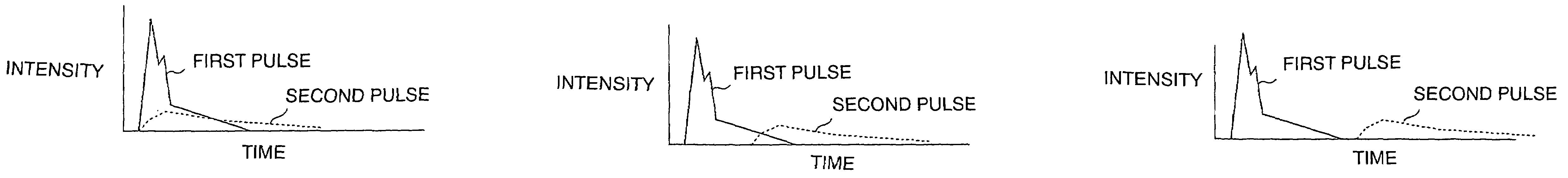
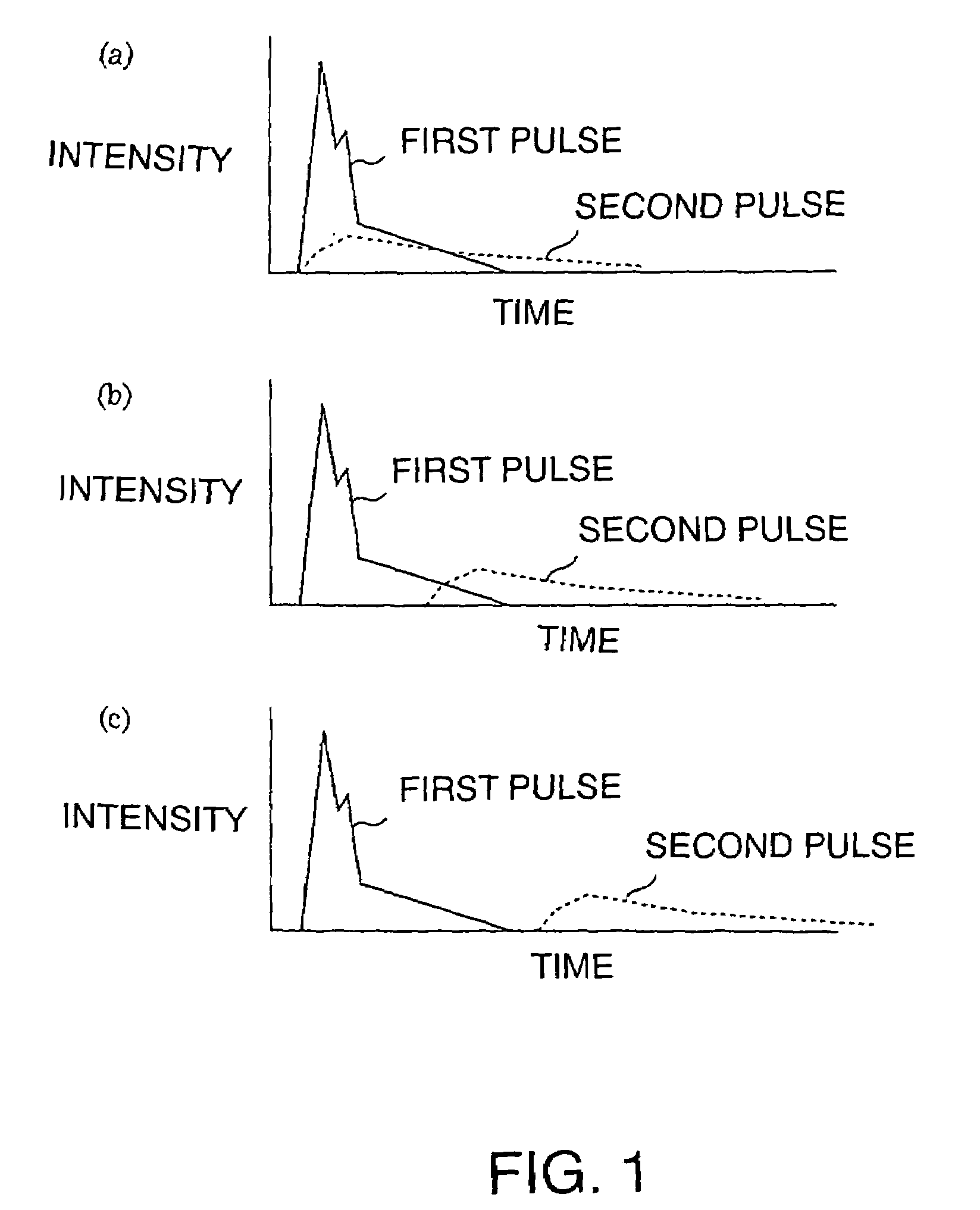
[0069]FIG. 1 illustrates an example of the embodiment of the present invention. Each of the oscillation start timings is depicted on the abscissa axis while the irradiation energy is depicted as the region bound by the pulse line. FIG. 1(a) shows an example where a first pulse laser and a second pulse laser are oscillated at the simultaneous timing. The time interval required between the supply of the trigger signal for controlling the oscillation and the actual start of the oscillation often depends upon the construction of the laser apparatus. Therefore, the “trigger oscillation” time is predetermined so that the irradiation can be simultaneously carried out. Since the emission time of the second pulse is longer than that of the first pulse, the gradual-cooling effect becomes higher during the melting and solidifying process. Moreover, during the melting process by the first pul...


PUM


Abstract

A thin film processing method for processing the thin film by irradiating an optical beam to the thin film. A unit of the irradiation of the optical beam includes a first and a second optical pulse irradiation to the thin film, and the unit of the irradiation is carried out repeatedly to process the thin film. The first and the second optical pulse have pulse waveforms different from each other. Preferably, a unit of the irradiation of the optical beam includes the a first optical pulse irradiated to the thin film and a second optical pulse irradiated to the thin film starting substantially simultaneous with the first optical pulse irradiation. In this case, the relationship between the first and the second optical pulse satisfies (the pulse width of the first optical pulse)<(the optical pulse of the second optical pulse) and (the irradiation intensity of the first optical pulse)≧(the irradiation intensity of the second optical pulse). A silicon thin film with a small trap state density can be formed by the optical irradiation.

Description

BACKGROUND OF THE INVENTION[0001]1. Field of the Invention[0002]This invention relates to a system for the formation of a silicon thin film and a good-quality semiconductor-insulating film interface. Such silicon thin films are used for crystalline silicon thin film transistors, and such semiconductor-insulating film interfaces are employed for field effect transistors. The invention also relates to a semiconductor thin film forming system by the pulsed laser exposure method. In addition, the invention relates to a system for the manufacture of driving elements or driving circuits composed of the semiconductor thin films or field effect thin film transistors for displays and sensors, for example.[0003]2. Description of the Related Art[0004]Typical processes for the formation of a thin film transistor (TFT) on a glass substrate are a hydrogenated amorphous silicon TFT process and a polycrystalline silicon TFT process. In the former process, the maximum temperature in a manufacture pr...

Claims


Application Information

Patent Timeline
IPC IPC(8): H01L21/44H01L21/48H01L21/50H01L21/76H01L21/20H01L21/208H01L21/268H01L21/336H01L29/786
CPCH01L21/02532H01L21/0262H01L21/02686H01L21/268H01L29/66757H01L29/78675H01L21/31
Inventor TANABE, HIROSHITANEDA, AKIHIKO
Owner NEC CORP
Why Eureka
Try Eureka