Electro-optical modulating display and method of making the same

a technology of optical modulation and display, applied in the direction of discharge tube luminescnet screen, instruments, heat measurement, etc., can solve the problems of difficult to adjust the thickness of the seal, difficulty in preventing or minimizing the degree of intermixing between the sealing, and difficulty in forming partitions. to achieve the effect of enhancing contras

Inactive Publication Date: 2008-01-29
EASTMAN KODAK CO
View PDF13 Cites 23 Cited by
  • Summary
  • Abstract
  • Description
  • Claims
  • Application Information

AI Technical Summary

Benefits of technology

[0025]wherein the bead of excess fluid is allowed to flow widthwise beyond the boundary of the array of microcells in the first elongated sheet, thereby preventing the entrapment of air in the microcell reservoirs as they are sealed by the second elongated sheet during lamination.
[0028]The simultaneous sealing of the microcells and the side edges is advantageous for controlling or preventing excessive lateral spread of the excess electro-optical imaging fluid along the rolling bead. The simultaneous sealing or closure of the side edges causes sufficient electro-optical imaging fluid to move in the machine direction versus the side direction and contributes to fill uniformity. Thus, the microcells being sealed are uniformly filled with sufficient electro-optical imaging fluid. In a particularly preferred embodiment, the first sheet comprises, on each side thereof of, in parallel, a boundary area between the outer boundary of the array of microcells and the outer edge of the first sheet; so that the second sheet entering the nip extends widthwise beyond the array of microcells and within the boundary area of the first sheet, and the outer edges of the second sheet are bonded to the first sheet in the boundary area simultaneously with the sealing of the array of microcells during lamination. The first sheet can comprise patterned electrodes and, along the edge of the boundary areas, contacts for the patterned electrodes, in which case the edges of the second sheet preferably does not extend as far as the contacts, and the contacts are left uncovered by the second sheet when the sides of the second sheet are bonded to the first sheet in the boundary area during lamination.
[0036]Yet another aspect of the present invention relates to a an electro-optical display comprising an array of microcells sealingly filled with an electro-optical imaging fluid that comprises charged particles dispersed in a carrier fluid that is a transparent or colored organic dielectric fluid comprising a long chain hydrocarbon or paraffin, optionally halogenated, in which an integral second sheet is laminated to a first sheet, which integral second sheet comprises an adhesive layer over a support, the integral second sheet sealing each of the filled microcell reservoirs in the array by the adhesive layer adhesively bonding to the tops of the side walls of each microcell reservoir in the array, wherein the adhesive layer comprises a non-ionic polymeric material that is substantially insoluble in said organic dielectric fluid and capable of bonding the integral second sheet to the top of the side walls of the microcell reservoirs even when covered or wetted with the organic dielectric fluid. This adhesive material is particularly advantageous when electro-optical display has been manufactured by a method involving sealing microcells containing a slight excess of carrier fluid to prevent bubble entrapment during sealing, causing the wetting of the tops of the side walls with the dielectric fluid. A superior adhesive material for achieving this purpose is a polyester-type thermoplastic polyurethane (TPU) or an amorphous or semi-crystalline copolyester resin.

Problems solved by technology

However, in the case of partition-type electrophoretic displays, difficulties were encountered in the formation of the partitions, in the process of enclosing the fluid suspension, and in the case of colored displays, in segregating different colored fluid suspensions from each other in partition-type electrophoretic displays.
Notably, the sealing composition is immiscible or otherwise incompatible with the solvent and has a lower specific gravity than the solvent and pigment particles.
Among the problems with this type of sealing arrangement are difficulties in preventing or minimizing the degree of intermixing between the sealing composition and the pigment dispersion.
Also, it is difficult to adjust the thickness of the seal, which needs to be much less than that of the electrophoretic fluid in order to provide the necessary optical density.
Consequently, the specific gravity and viscosity of the materials must be carefully controlled, which limits the materials that can be used.
However, this adds complexity and further steps to the fabrication process.
Ukigaya states that production steps and apparatus for forming the adhesive layer are complicated and can cause yield reductions or increased production costs.
This type of approach may prove useful for some types of electrophoretic cell design, but would offer no advantage for an in-plane electrode design, in which all electrodes lie in the same plane within the electrophoretic cell.
Also, the requirement for electrical conductivity of the adhesive significantly narrows the choices of adhesive material available, and steps taken to provide or enhance resin conductivity using metallic powders or other particulates could cause disadvantageous optical effects in the display.
However, Doshi et al. do not describe how to laminate a backplane to an unsealed microcell sheet containing a flowable liquid fluid as compared to a dried, coherent layer.
Doshi et al. also disclose the use of vacuum lamination; however, this would be inappropriate with liquid or other materials that are not already bonded to an underlying substrate in some way.
Daniel et al., however, point out disadvantages of applying a continuous layer of adhesive onto a substrate for bonding to cell walls for sealing the electrophoretic microcells.
Notably, excess liquid adhesive that is not used in forming the bond with the wall microstructure of the microcells tends to migrate into or otherwise intermix with the contents of the cells.
This unwanted mixing can undesirably affect properties of the electrophoretic substance contained within the cells.
Thus, while this type of approach may prove useful for some cell sealing applications, there are drawbacks and limitations to such a solution for the broad range of electrophoretic and other electro-optical modulating image-forming applications.
In view of the above, conventional approaches for sealing an array of microcells in an electro-optical modulating display have not provided solutions that are sufficiently adaptable and robust for large-scale production.
Among the problems that have not been adequately addressed are difficulties due to the composition of the electrophoretic fluid itself.
Many of the liquids and solvents used can even prove inimical to conventional surface adhesion materials and techniques or, at best, allow only marginal performance.
Self-capping approaches such as those taught by Liang et al. and elsewhere place constraints on both the electrophoretic composition and on the sealing materials themselves.
The adhesive electrode taught in the Ukigaya disclosure allows only a narrow range of materials and is not appropriate for designs using an in-plane electrode layout.
The method of Doshi et al., involving lamination, may be suitable for electrophoretic composite materials that are not fluid in nature, but do not satisfy the more demanding requirements posed by microcells containing a liquid electrophoretic medium.
Finally, adhesive capsules as proposed by Daniel et al. allows only a narrow range of adhesives, may pose limitations due to cost and suitability for mass manufacture, and may result in a residue of material in the microcells that can adversely effect optical performance.
Still another problem with sealing an array of microcells, particularly when simultaneously laminating and sealing an array of liquid-containing microcells is to prevent or limit the entrapment of any air while sealing the microcells, since air bubbles formed in sealed microcells will result in undesirable variations in image density among the microcells.

Method used


Image

  • Electro-optical modulating display and method of making the same
  • Electro-optical modulating display and method of making the same
  • Electro-optical modulating display and method of making the same

Examples


Embodiment Construction

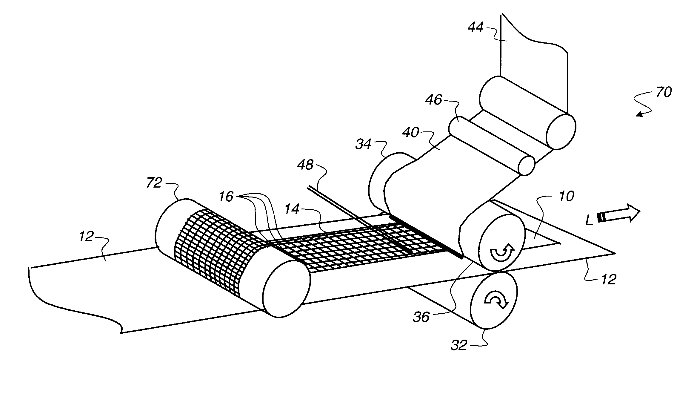
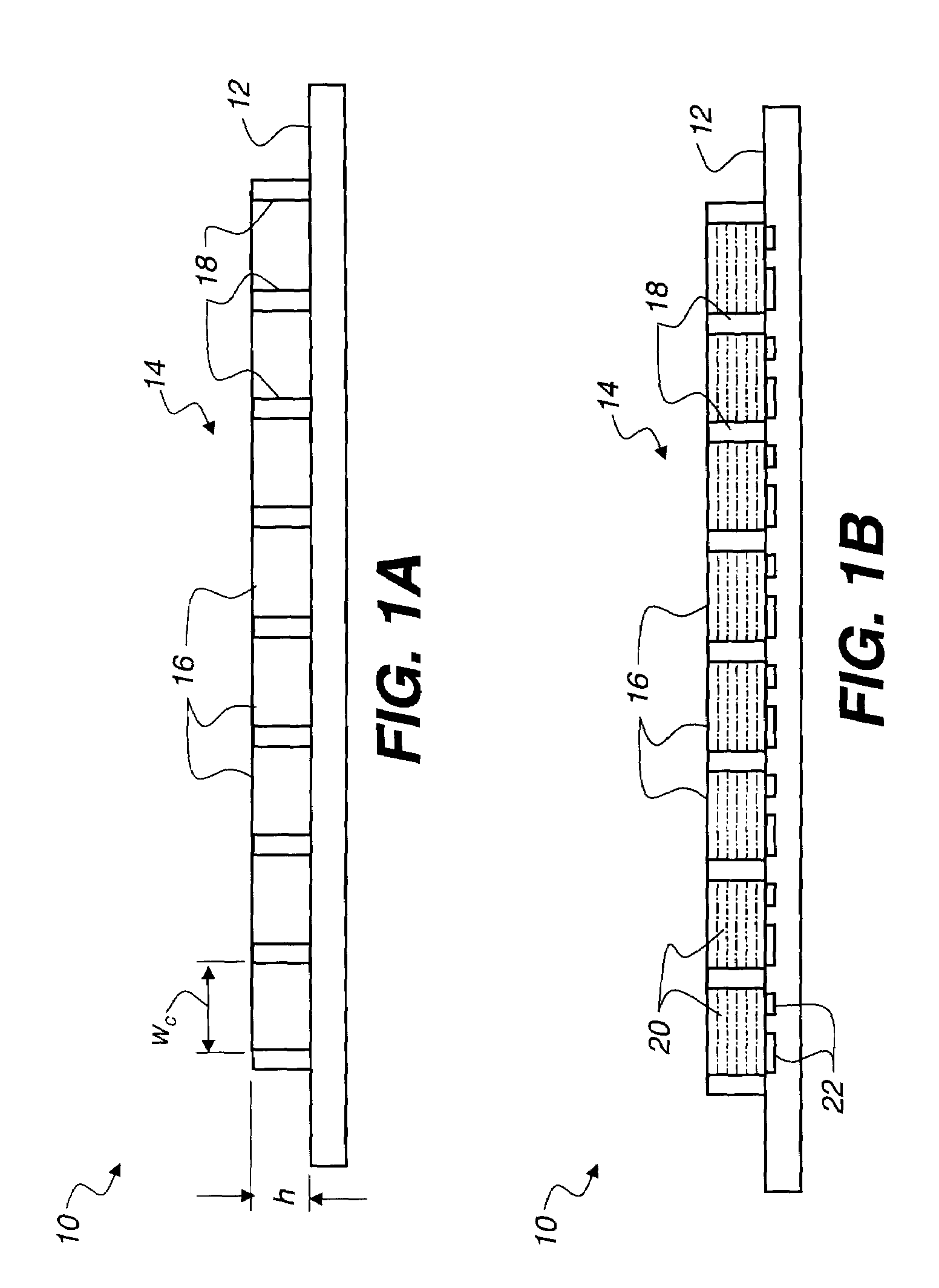
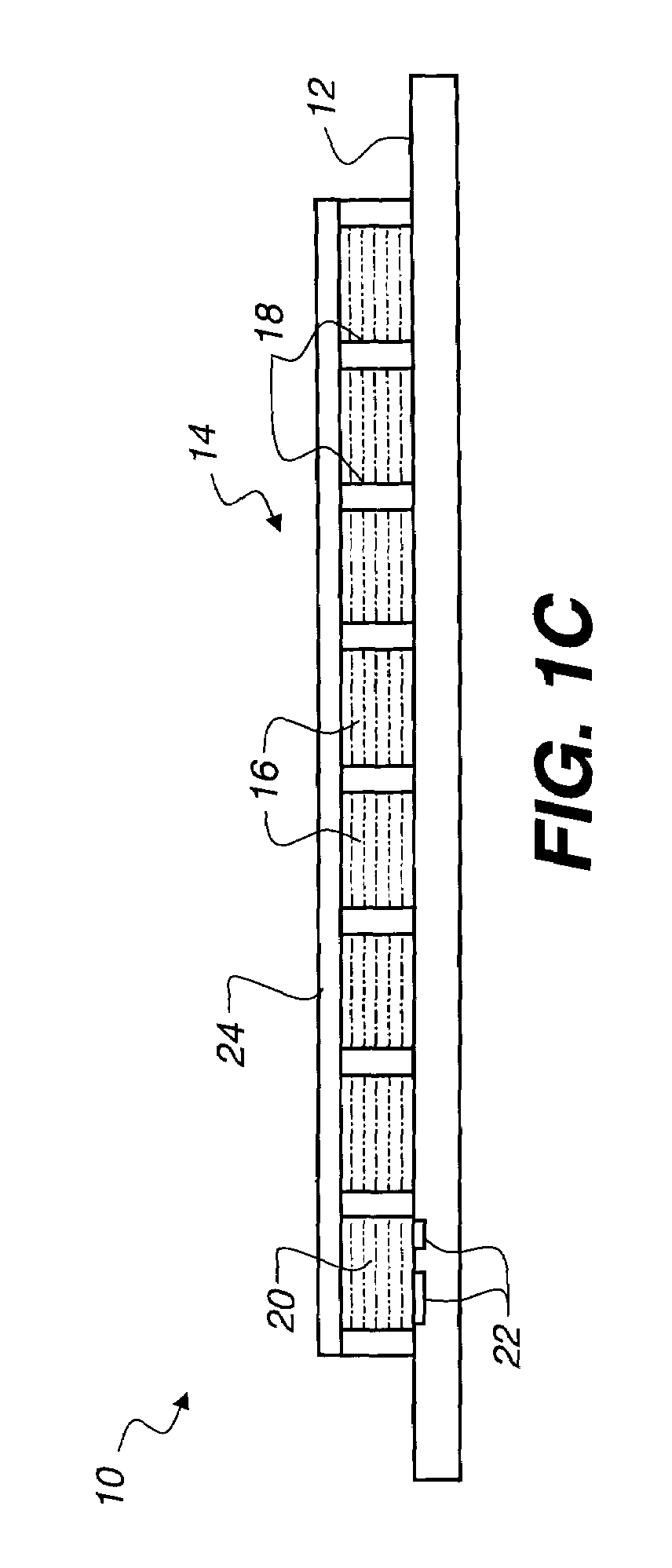
[0056]As indicated above, the present invention is directed to a method of manufacturing an array of microcells. In one embodiment, the present invention relates to a method of making a display device comprising a substrate or support, a patterned conductor, and an electro-optical imaging fluid. The electro-optical imaging fluid used in the present invention is a light modulated liquid fluid, and can be reflective or transmissive. Such light modulating fluid materials can be electrochemical, electrophoretic, or electrochromic, or may comprise particles such as GYRICON particles or liquid crystals. The preferred light-modulating fluid for an imaging layer comprises an electrophoretic material.

[0057]For the imaging device made by the present invention, a preferably flexible support substrate bears an electrically modulated imaging layer over at least one surface. As used herein, the terms “over,”“above,”“on,”“under,” and the like, with respect to layers in the display element, refer t...


PUM

PropertyMeasurementUnit
widthaaaaaaaaaa
thicknessaaaaaaaaaa
temperatureaaaaaaaaaa

Abstract

This invention relates to a method of manufacturing micro-cell arrays. Such an array may find use in a number of applications such as, for example, a video display, electronic paper, and signage. The microcell arrays find particular use in electromodulating displays.

Description

FIELD OF THE INVENTION[0001]The present invention relates generally to the field of electro-optical modulating displays, for example, electrophoretic displays and, specifically, to a novel method of manufacturing such displays. In particular, the invention relates to novel electro-optical modulating display structure and methods of sealing liquid-based imaging material in microcells associated with such electro-optical modulating displays.BACKGROUND OF THE INVENTION[0002]The electrophoretic display offers an electronic alternative to conventional printed-paper media for many applications. The electrophoresis phenomenon is based on charged particles suspended in a liquid fluid, for example charged pigment particles in an organic solvent. Unlike sheet materials containing magnetic memory areas that can be written electronically, an electrophoretic display advantageously provides a visible record for the viewer.[0003]Electrophoretic media systems exist that maintain electronically chan...

Claims


Application Information

Patent Timeline
Patent Type & Authority Patents(United States)
IPC IPC(8): G02B26/00G02F1/01G09G3/34G02F1/167G02F1/1679G02F1/1681
CPCG02F1/167G02F2001/1672G02F1/1681G02F1/1679
Inventor AYLWARD, PETER T.SMITH, THOMAS M.GATES, LEONARD S.SLATER, DANIEL A.
Owner EASTMAN KODAK CO
Why Eureka
Try Eureka