Non-volatile memory architecture employing bipolar programmable resistance storage elements

a programmable resistance and memory architecture technology, applied in the field of memory devices, can solve the problems of increasing the complexity, increasing the cost of memory cells, directly proportional to memory cell size, etc., and achieves the effect of minimizing the footprint of the device, increasing the complexity of peripheral support circuits associated, and efficient memory array layou

Active Publication Date: 2008-01-29
GLOBALFOUNDRIES US INC
View PDF7 Cites 42 Cited by
  • Summary
  • Abstract
  • Description
  • Claims
  • Application Information

AI Technical Summary

Benefits of technology

[0005]The present invention meets the above-noted need by providing, in an illustrative embodiment, a nonvolatile memory array employing bipolar programmable resistance elements which is configured to enable direct write operation and thereby eliminate the need for an intervening erase operation, without increasing a complexity of peripheral support circuits associated with the memory array. A device utilizing this memory array may be fabricated in a manner which minimizes a footprint of the device, so as to achieve an efficient memory array layout.

Problems solved by technology

This intervening erase operation undesirably increases the complexity of circuits that are peripheral to the memory device in order to support the generation of the negative voltages employed, and is therefore an impediment to achieving higher performance in the memory device.
Consequently, the cost of the memory cell, which is directly proportional to memory cell size, would increase accordingly.

Method used


Image

  • Non-volatile memory architecture employing bipolar programmable resistance storage elements
  • Non-volatile memory architecture employing bipolar programmable resistance storage elements
  • Non-volatile memory architecture employing bipolar programmable resistance storage elements

Examples


Embodiment Construction

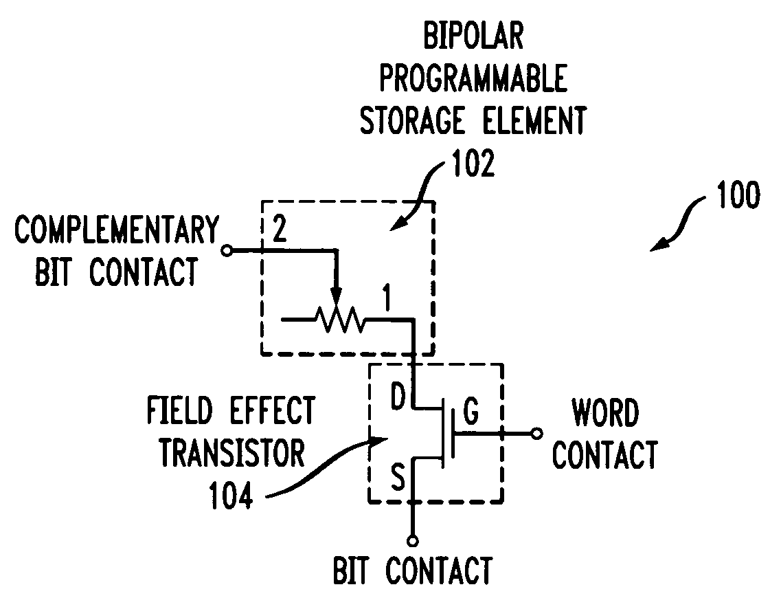
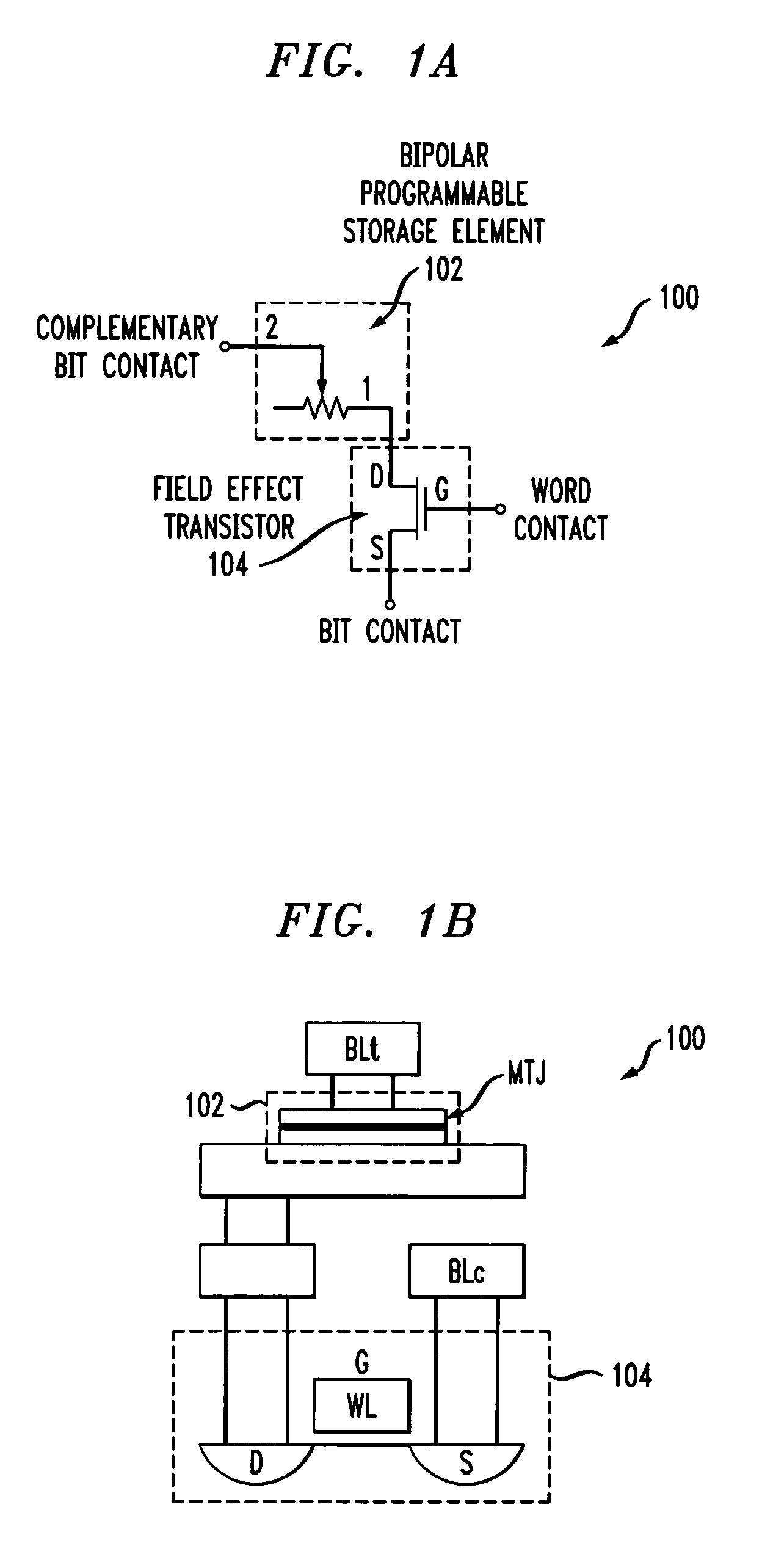
[0015]The present invention will be described herein in the context of an illustrative nonvolatile memory cell and a memory array employing a plurality of such nonvolatile memory cells. It should be understood, however, that the present invention is not limited to these or any other particular circuit arrangements. Rather, the invention is more generally applicable to techniques for enhancing a programming performance of a nonvolatile memory array employing memory cells comprising bipolar programmable resistance elements. Although implementations of the present invention are described herein with specific reference to a metal-oxide-semiconductor (MOS) field-effect transistor (FET) device, as may be formed using a complementary metal-oxide-semiconductor (CMOS) fabrication process, it is to be understood that the invention is not limited to such transistor devices and / or such a fabrication process, and that other suitable devices, such as, for example, bipolar junction transistors (BJ...


PUM


Abstract

A nonvolatile memory array includes a plurality of word lines, a plurality of bit lines, a plurality of source lines, and a plurality of nonvolatile memory cells. Each of at least a subset of the plurality of memory cells has a first terminal connected to one of the plurality of word lines, a second terminal connected to one of the plurality of bit lines, and a third terminal connected to one of the plurality of source lines. At least one of the memory cells includes a bipolar programmable storage element operative to store a logic state of the memory cell, a first terminal of the bipolar programmable storage element connecting to one of a corresponding first one of the bit lines and a corresponding first one of the source lines, and a metal-oxide-semiconductor device including first and second source / drains and a gate. The first source / drain is connected to a second terminal of the bipolar programmable storage element, the second source / drain is adapted for connection to a corresponding second one of the bit lines, and the gate is adapted for connection to a corresponding one of the word lines. For at least a subset of the plurality of memory cells, each pair of adjacent memory cells along a given word line shares either the same bit line or the same source line.

Description

FIELD OF THE INVENTION[0001]The present invention relates generally to memory devices, and more particularly relates to a nonvolatile memory architecture employing a bipolar programmable resistance element.BACKGROUND OF THE INVENTION[0002]Storage elements employing bipolar programmable resistance materials offer a potential replacement for current non-volatile memory, including, but not limited to, flash memory, one-transistor one-capacitor (1T1C) dynamic random access memory (DRAM) and static random access memory (SRAM). Memory devices employing bipolar programmable resistance storage elements typically rely on a reversal of the polarity of a voltage applied across the storage element in each of the devices in order to write the respective logic states of the memory devices. These nonvolatile bipolar programmable resistance storage elements, which include materials such as “spin-switched” or “spin momentum transfer” magnetic materials and / or programmable resistance transition-metal...

Claims


Application Information

Patent Timeline
Patent Type & Authority Patents(United States)
IPC IPC(8): G11C11/00
CPCG11C8/14G11C11/16G11C11/1655G11C11/1657
Inventor BEDNORZ, JOHANNES GEORGLAM, CHUNG HONMEIJER, GERHARD INGMAR
Owner GLOBALFOUNDRIES US INC
Why Eureka
Try Eureka