
Analog built-in self-test module

a built-in, self-testing technology, applied in the direction of individual semiconductor device testing, error detection/correction, instruments, etc., can solve the problems of inability to purchase, inability to test devices, and the limitations of speed and performance of most testers, so as to improve testing capacity, fast analog final test and analog characterization, the effect of improving the flexibility of component specifications

Active Publication Date: 2008-02-05
TEXAS INSTR INC
View PDF1 Cites 65 Cited by
  • Summary
  • Abstract
  • Description
  • Claims
  • Application Information

AI Technical Summary

Benefits of technology

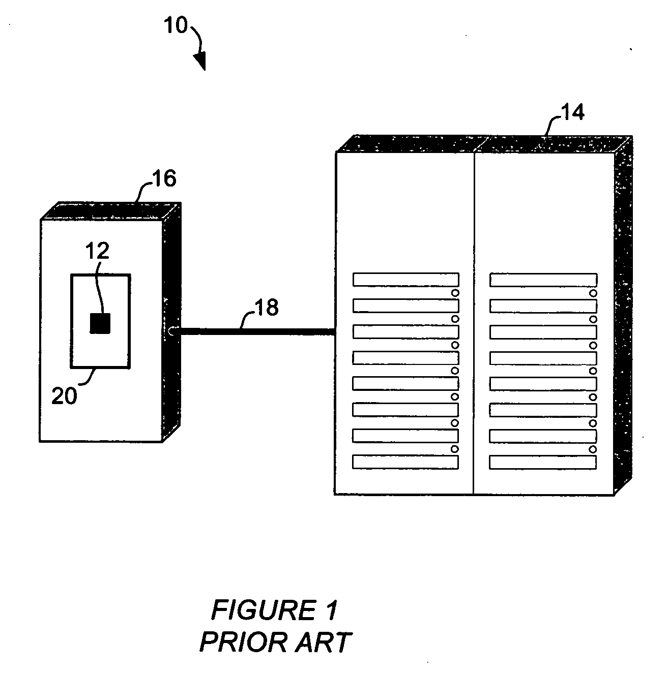
[0012]In the present invention, a tester connects to a test interface board, called a “load board, that is attached to a test head. One side of the load board has a socket that receives an integrated circuit chip for analog testing. The opposite side of the board contains all the electrical connections, circuitry, chips, and processors needed for performing the test on the chip. The improvement to this system comprises additional electronic circuitry that is designed into or attached to the load board that performs the tasks of a test formerly performed by a tester 14. The circuitry is organized on a board called an analog BIST (Built-in Self Test) module. On the test module, analog circuits are attached to the load board that perform most, or all, of the testing tasks. The analog tests can be performed by one or more test boards on a load board in parallel for one or multiple devices under test (DUTs), resulting in faster testing than a conventional tester.
[0013]If a tester can perform one analog test, one device at a time and each test takes one second, about 100 seconds are required for testing one hundred analog cells in a single DUT. But on the load board, with specific circuitry of a test module to test one hundred analog circuits in parallel, the entire test takes one second, significantly increasing efficiency of device testing and reducing costs. In production of an integrated circuits, millions of chips may be produced and tested. The savings of millions of seconds of test time provided by the present invention also reduces the costs an equivalent amount.
[0014]Conventional testers are very expensive and cannot be purchased often to keep up with the fastest computer technology. Most testers have built-in limitations of speed and performance to test devices. For example, if input bandwidth of the analog measurement unit on the tester is limited to 100 MHz, the test module of the present invention can be built to a specified input bandwidth of 500 MHz or 1 GHz. It is much easier and cost effective to replace a component of a load board in order to increase processing speed and capacity of a test system instead of either putting an expensive production run on hold or to buy a completely new test system.
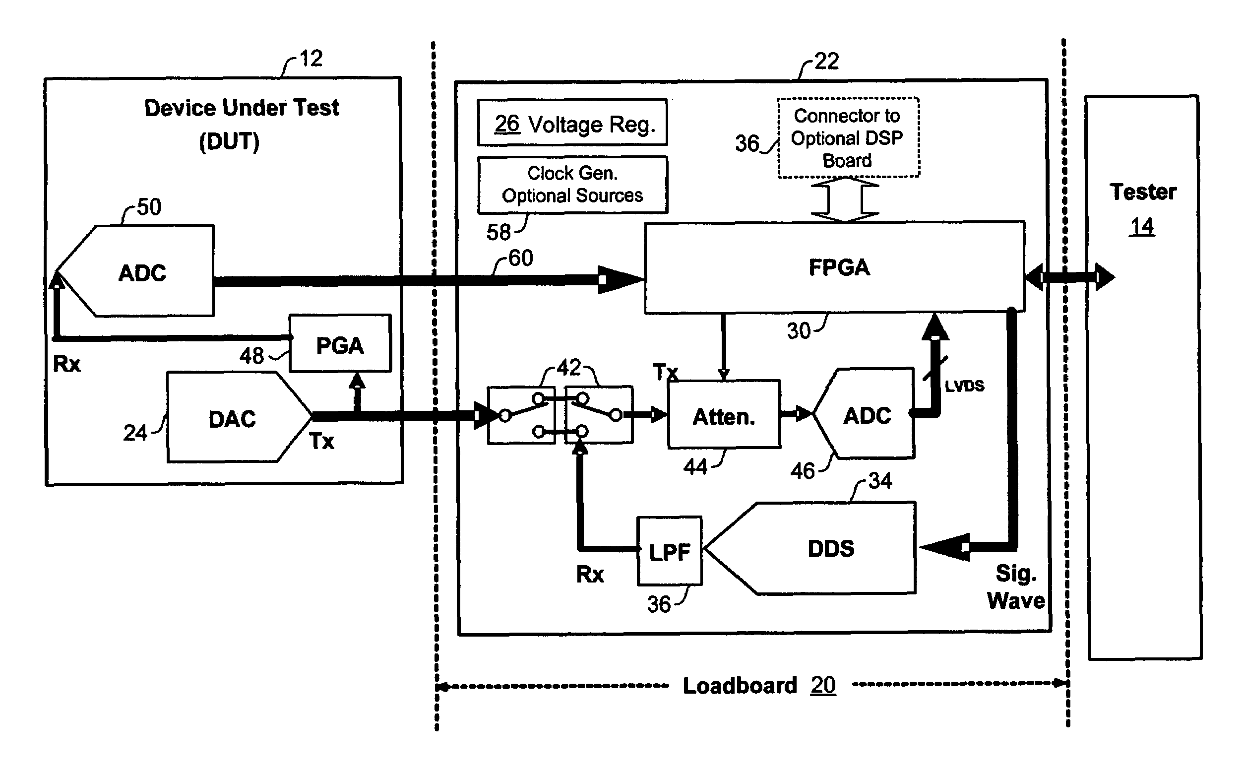
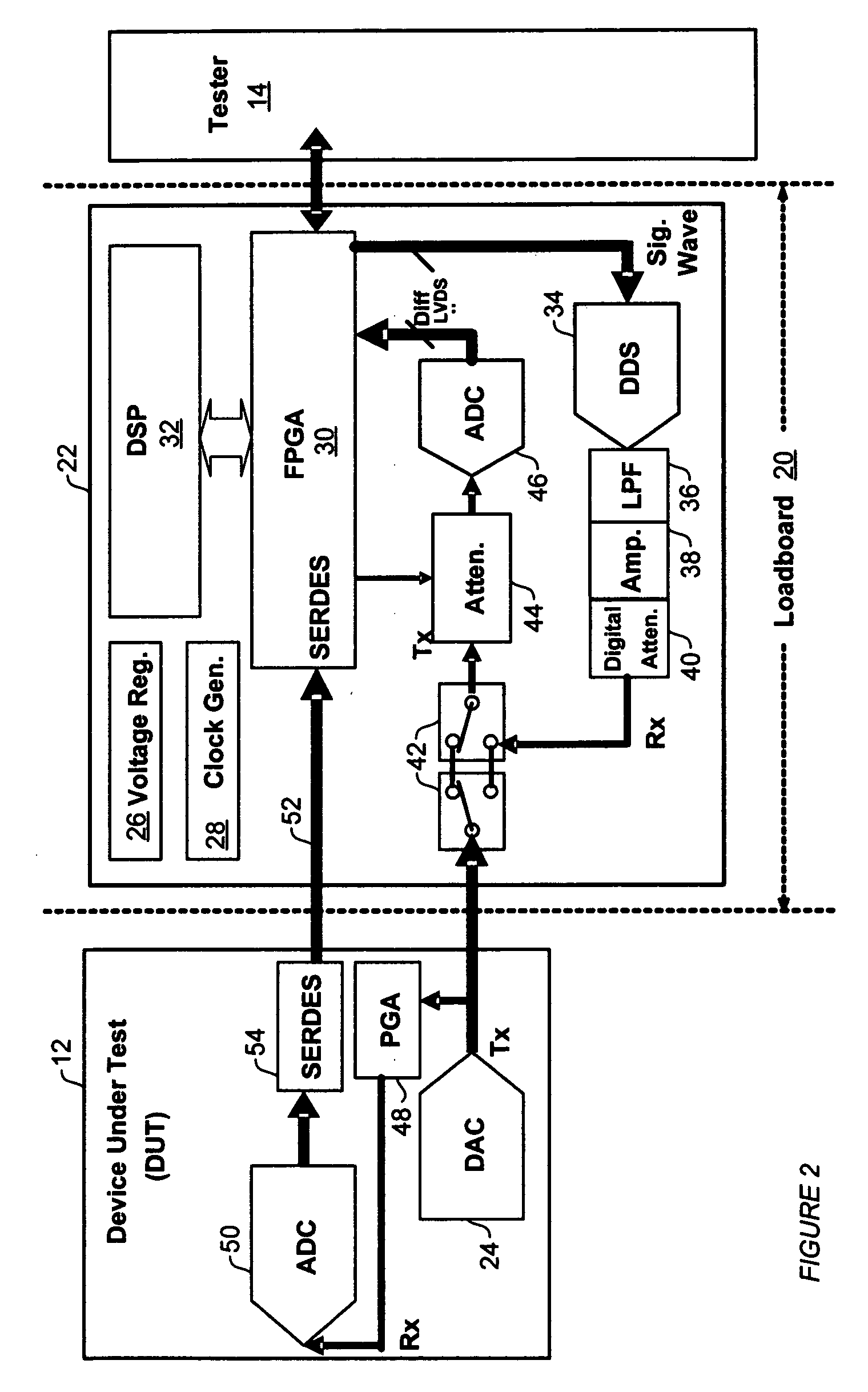
[0016]To increase flexibility of component specifications and testing capacity, the exemplary analog BIST module of the present invention is preferably an add-on component to a load board, however the load board itself could have the components and functionality of a test module built-into the board. Components of a test module include an FPGA (Field Programmable Gate Array). Test setup is performed by the FPGA. A DAC or DDS is used to drive any analog input of the DUT and an amplifier may be added in the stream with a digital attenuator to adjust the test signal amplitude. Test data inside the DUT that is converted to digital by an ADC (Analog-to-Digital Converter) is exported through an optional SERDES (serialize / deserialize) port. The FPGA captures the test data from the SERDES into memory or a buffer and drives the data to an on-board DSP for analysis. An ADC with a high input band-width samples or under-samples any analog output from the DUT prior to export in digital format to the FPGA. The processing and speed for analyzing the captured data may be adjusted by choosing the appropriate number of DSPs for the volume and type of tests being performed on multiple DUTS in a tester. Relays are also included in the test module to enable self-test of the BIST prior to starting device tests and to apply / measure Analog differential signals to / from the DUT.
[0017]The various embodiments of an analog BIST module enable extremely fast analog final test and analog characterization of a DUT on any tester, such as a VLCT. Test setup can be performed simpler and faster by DFT (Design for Test) techniques so that every test mode will set a value into all relevant registers inside the DUT without the need for programming by functional vectors. The module enables parallel, simultaneous tests of all analog ports or differential channels of the DUT. The jitter in the clock distribution on the module is reduced by using OCXO and LVPECL devices and level translators for every clock receiver. Data stimuli and capture is performed faster by using high-speed digital interfaces such as SERDES and LVDS, and ADC or DAC / DDS components with appropriate speed specifications. Data analysis is performed quicker by using one or more DSPs on the module without functional patterns for transferring the captured data to the tester. Various implementations of the analog BIST module in a test system include directly attached to a load board, connected to a load board through an appropriate data bus.

Problems solved by technology

Conventional testers are very expensive and cannot be purchased often to keep up with the fastest computer technology.
Most testers have built-in limitations of speed and performance to test devices.

Method used


Image

  • Analog built-in self-test module
  • Analog built-in self-test module
  • Analog built-in self-test module

Examples


Embodiment Construction

[0030]The preferred exemplary embodiment of the present invention includes an external analog built-in self-test (BIST)module for a test interface board, such as a load board on a test head, for testing devices such as integrated processors (IC). Analog BIST is from perspective of the test board or Tester and not the device under test. Built in self test, which is called a BIST is usually a reference for something that is internal to the DUT. But for this application, when I am building a test board, I mean that it is a BIST on the board and the board is doing the work instead of the tester. So from the tester point of view, it is a BIST on the load board, which is called the test board or the load board for production.

[0031]FIG. 2 illustrates a block diagram of a preferred embodiment of an analog BIST module 22 and operative connections and divisions between the preferred module 22, a device under test (DUT) 12, and a tester 14 of a system for testing IC devices. The diagram shows ...


PUM


Abstract

An analog BIST (Built-in Self-Test) module for a load board in a test system for testing Integrated Chips (IC) and other devices-under-test (DUTs). Components of the test module perform test setup, transmission of analog test signals to a DUT, capture of analog and digital test data from the DUT, and on-board analysis of the test data using DSPs without sending the test data to a tester. Modules may be add-on boards to load boards an contain one or more processors and multiple components to test DUTs in parallel, significantly decreasing test and analysis times of a test system such as a Very Low Cost Tester (VLCT).

Description

CROSS-REFERENCE TO RELATED APPLICATIONS[0001]NoneFIELD OF THE INVENTION[0002]This invention relates generally to automatic test equipment used to test integrated circuit elements, and more particularly to interface hardware used in automatic test equipment to connect devices under test to a test head in order to perform the testing.BACKGROUND OF THE INVENTION[0003]Automatic test equipment is generally used to test semiconductor devices and integrated circuit (IC) elements, such as memory or logic, for manufacturing defects. Manufacturers of automatic test equipment (ATE) offer test systems to address the increasingly complex task of testing advanced ICs. However, many commercially available ATE systems are complex, proprietary, not easily flexible to meet changing test conditions, and often require additional heat removal systems and typically cost several million dollars that make them unattractive for use in a cost driven manufacturing environment. Recently, many semiconductor man...

Claims


Application Information

Patent Timeline
Patent Type & Authority Patents(United States)
IPC IPC(8): G01R31/02G06F11/00
CPCG01R31/3167G01R31/31917
Inventor WEINRAUB, CHANANIEL
Owner TEXAS INSTR INC
Learn More