Array testing method using electric bias stress for TFT array

a thin film transistor and array technology, applied in the testing of individual semiconductor devices, static indicating devices, instruments, etc., can solve the problems of deteriorating the image quality of tft-lcd during operation, inability to move charges (off current), and unstable amorphous silicon, etc., to reduce the overall cost

Active Publication Date: 2008-02-05
ORBOTECH LTD
View PDF8 Cites 6 Cited by
  • Summary
  • Abstract
  • Description
  • Claims
  • Application Information

AI Technical Summary

Benefits of technology

[0018]The defect detection may be applied at the TFT fabrication level to screen defective plates prior to assembly into modules. The defect detection is performed at an early stage in the process and thus reduces the overall costs.

Problems solved by technology

However, In the case of defective TFTs, the off-current variation with temperature is large enough to deteriorate the TFT-LCD image quality during operation.
Amorphous silicon is not very stable and its properties can be modified when exposed to strong illumination or injection of charge carriers.
The dangling bonds are defects within the amorphous semiconductor layer and contribute to a nonzero density of states within the band gap, thereby resulting in the mobility of charges (off current).
During processing, however, the Si:H bond can be inadvertently broken.
Generation of high energy ions during processing can be due to poor or incorrect process parameters, and may result in a global plate (panel) effect rather than in a single, stand-alone TFT defect.
In other words, a whole area of a panel rather than a single isolated TFT may have poor quality a-Si:H film.
Recently, the TFT-LCD panel manufacturers have noticed at module assembly that the powerful (and therefore heating) backlights cause such defects and adversely affect the yield.
In practice, however, such a method is difficult to implement at the high throughput rates required by the TFT-LCD manufacturers.
The main drawbacks associated with heating full panels and measuring Ioff are (a) the time required to heat the panels and (b) the complexity of the apparatus needed to accommodate the large-sized panels, which may be two meters long, and two meters wide.

Method used


Image

  • Array testing method using electric bias stress for TFT array
  • Array testing method using electric bias stress for TFT array
  • Array testing method using electric bias stress for TFT array

Examples


Embodiment Construction

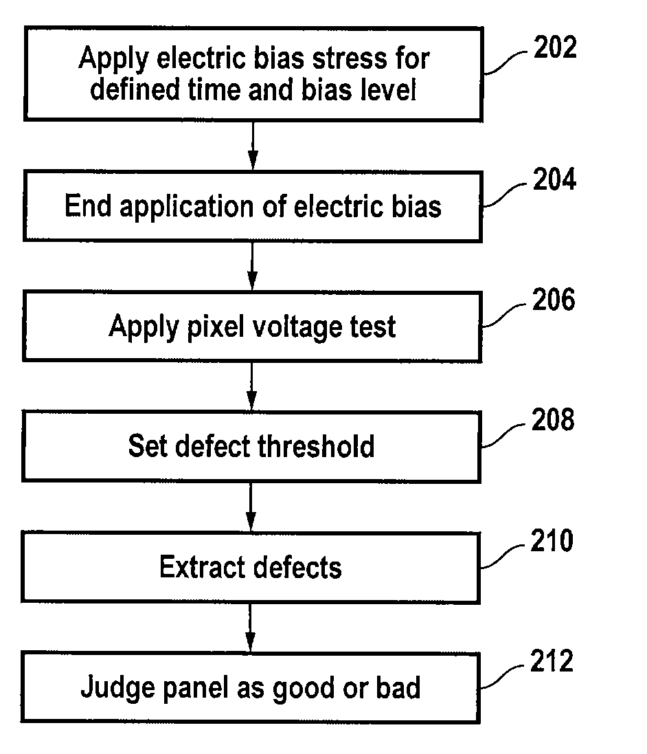
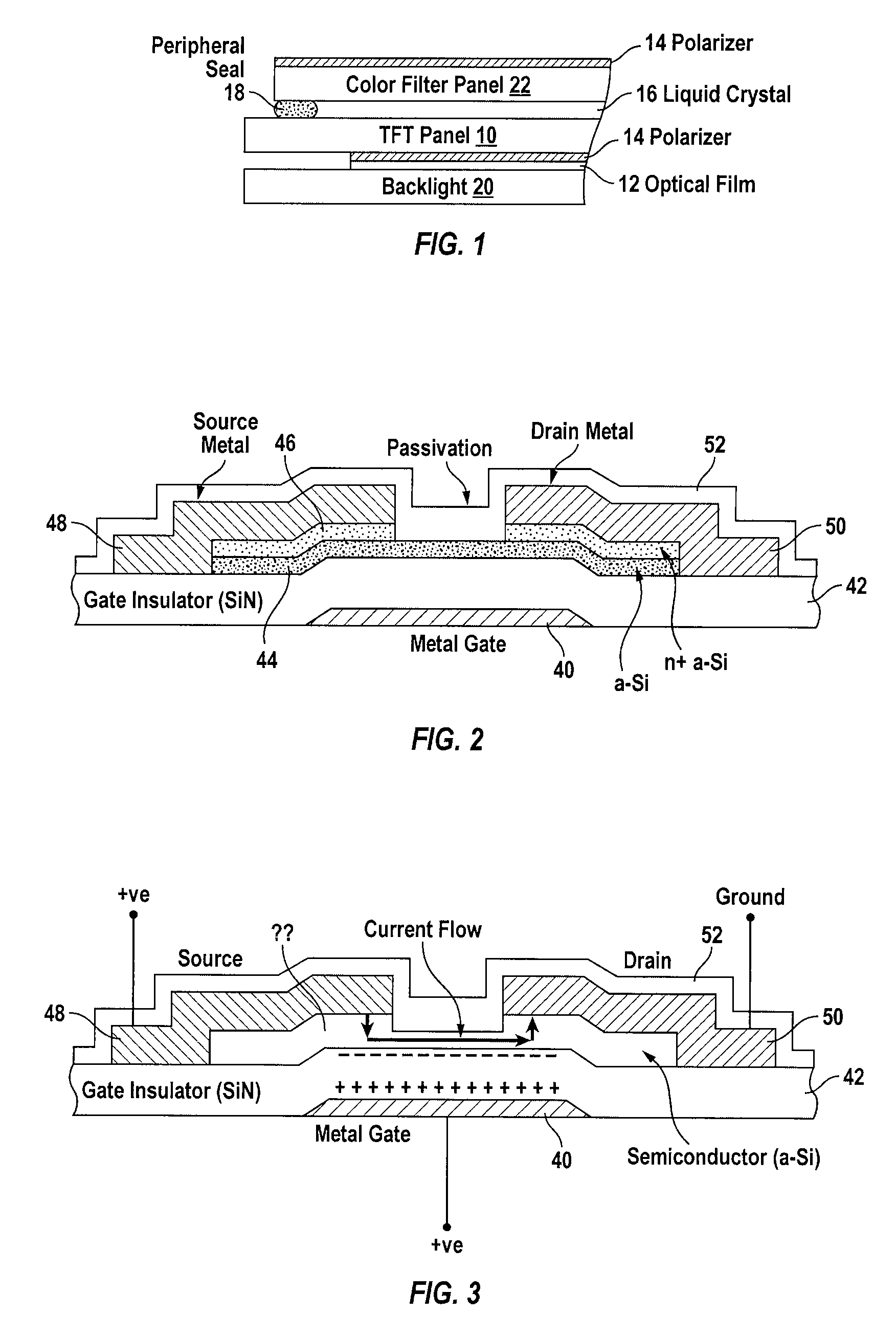
[0032]In accordance with the present invention, to detect defects in a TFT panel, an electric bias is applied to the TFT panel for a known time period. The applied electric bias induces charge trapping in the SiNx film and / or state creation in the a-Si:H film, thus giving rise to the TFT threshold voltage shift. The shift in the threshold voltage results in the variation of the TFT IOFF current. The amount of the threshold voltage shift (ΔVT) depends on the applied bias voltage, the duration of the bias, as well as the initial density of state in the films.

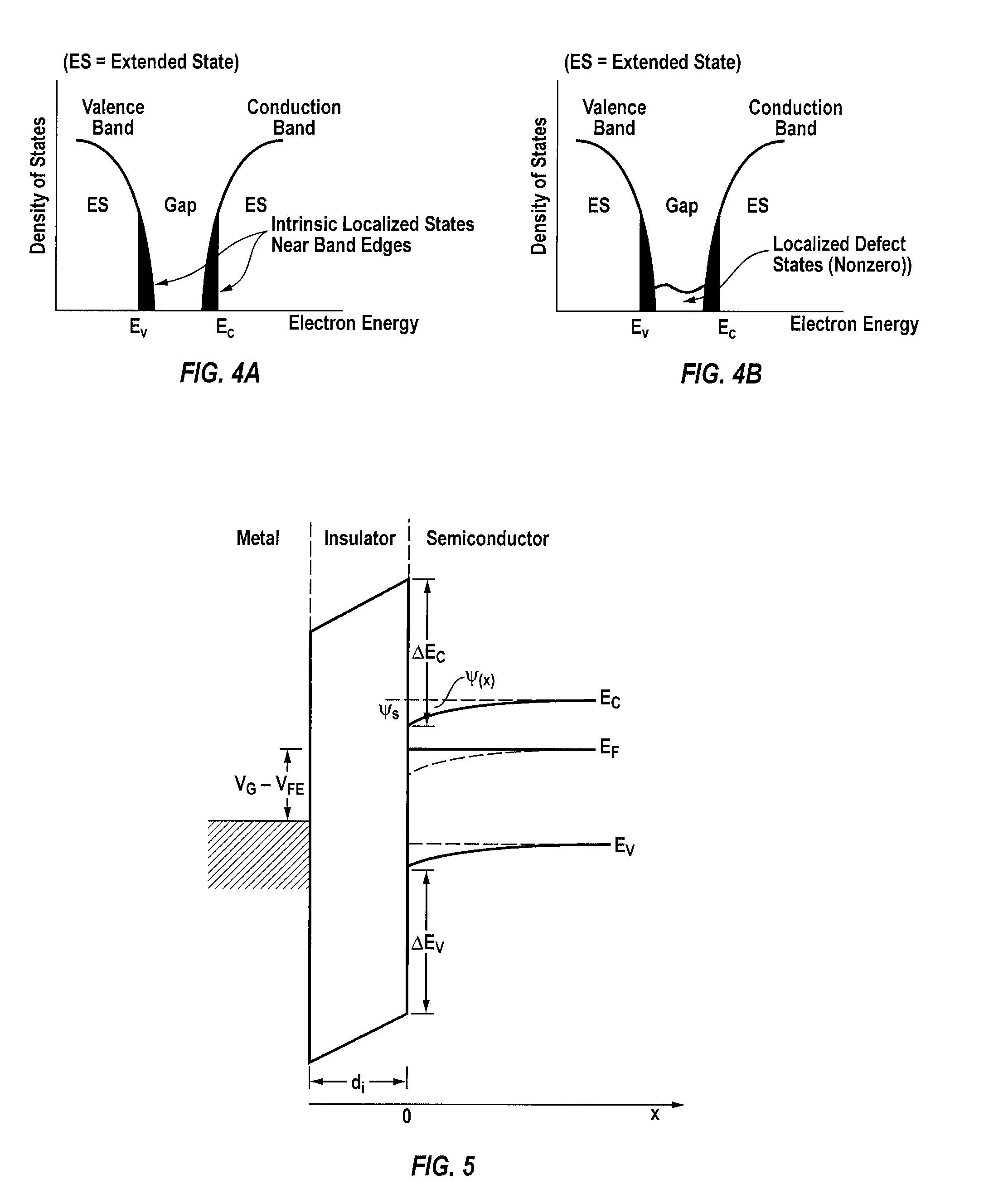
[0033]FIG. 7A is an energy band diagram of an MIS device prior to the application of an electric bias. FIG. 7B is an energy band diagram of the MIS device of FIG. 7A after the application of an electric bias causing charges to be trapped in the band gap. FIG. 7C is an energy band diagram of the MIS device of FIG. 7A after the application of an electric bias causing states to be created in the band gap.

[0034]FIG. 8 shows the depend...


PUM


Abstract

A method of detecting thin film transistor (TFT) defects in a TFT-liquid crystal display (LCD) panel, includes, in part, applying a stress bias to the TFTs disposed on the panel; and detecting a change in electrical characteristics of the TFTs. The change in the electrical characteristics of the TFTs may be detected using a voltage imaging optical system or an electron beam. The panel temperature may be varied while the bias stress is being applied. The change in the electrical characteristics is optionally detected across an array of the TFTs.

Description

BACKGROUND OF THE INVENTION[0001]The present invention relates to testing of thin film transistor (TFT) arrays, and more particularly to testing the functionality and reliability of such arrays.[0002]Thin film transistor liquid crystal displays (TFT-LCD) for, e.g., television applications require brighter backlight for better image quality. FIG. 1 is a cross-sectional view of a TFT-LCD module assembly. The stack includes a polarizer layer 14 and optical film 12, followed by the TFT panel 10 above which liquid crystal layer 16 is formed, and then the backlight 20. Color filter 22 and polarizer 14 are disposed above liquid crystal layer 16. Brighter backlight increases the temperature of TFT-LCD during operation, thus resulting in an increase in the TFT-LCD off current Ioff. For good TFTs, the variation in Ioff as a function of temperature is relatively small, and does not affect the TFT-LCD image quality. However, In the case of defective TFTs, the off-current variation with temperat...

Claims


Application Information

Patent Timeline
Patent Type & Authority Patents(United States)
IPC IPC(8): G01R31/00G01R31/26
CPCG09G3/006G09G2320/041G09G3/3648G02F1/13
Inventor JUN, MYUNGCHUL
Owner ORBOTECH LTD
Why Eureka
Try Eureka