MOS device for high voltage operation and method of manufacture

a high-voltage operation, mos technology, applied in the direction of semiconductor devices, electrical equipment, transistors, etc., can solve the problems of reducing the yield of integrated circuits, so as to achieve the effect of high device yield in dies per wafer and convenient us

Active Publication Date: 2008-02-26
SEMICON MFG INT (SHANGHAI) CORP
View PDF12 Cites 54 Cited by
  • Summary
  • Abstract
  • Description
  • Claims
  • Application Information

AI Technical Summary

Benefits of technology

[0008]In a specific embodiment, the invention provides a method for fabricating a high voltage semiconductor device. The method includes providing a substrate (e.g., silicon wafer) having a surface region. The method includes forming a well region within the substrate and forming a double diffused drain region within the well region. The method also includes forming a gate dielectric layer overlying the surface region and forming a gate polysilicon layer overlying the gate dielectric layer. A mask layer is formed overlying the gate polysilicon layer. The method includes patterning the gate polysilicon layer to form a gate electrode having a first predetermined width and a predetermined thickness. The gate electrode has a first side and a second side formed between the first predetermined width. The gate electrode is coupled to the double diffused drain region within the well region. Preferably, the first side has a lower corner overlying the gate dielectric layer and an upper corner underlying the mask layer and the second side has a lower corner overlying the gate dielectric layer and an upper corner underlying the mask layer. The method causes an oxidation of the gate electrode such that the lower corner on the first side and the lower corner on the second side convert from polysilicon material into silicon dioxide while the upper corner on the first side and the upper corner on the second side are substantially free from oxidation. The method continues to convert the lower corner of the first side and the lower corner of the second side to reduce the first predetermined with of the gate electrode comprising polysilicon material to a second predetermined width to increase a breakdown voltage of the high voltage semiconductor device to greater than 20 volts.
[0010]Many benefits are achieved by way of the present invention over conventional techniques. For example, the present technique provides an easy to use process that relies upon conventional technology. In some embodiments, the method provides higher device yields in dies per wafer. Additionally, the method provides a process that is compatible with conventional process technology without substantial modifications to conventional equipment and processes. Preferably, the invention provides for an efficient way of achieving high voltage applications, e.g., 20 volts and greater. Depending upon the embodiment, one or more of these benefits may be achieved. These and other benefits will be described in more throughout the present specification and more particularly below.

Problems solved by technology

An integrated circuit or chip fabrication facility can cost hundreds of millions, or even billions, of U.S. dollars.
Making devices smaller is very challenging, as each process used in integrated fabrication has a limit.
Additionally, as devices require faster and faster designs, process limitations exist with certain conventional processes and materials.
Smaller designs often cause lower voltages, which are undesirable for these types of integrated circuit devices.
Higher breakdown voltages are desired but are often at the expense of size, which limits the number of integrated circuits that can be fabricated on a single wafer.
Unfortunately, LDMOS structures are often larger in size.

Method used


Image

  • MOS device for high voltage operation and method of manufacture
  • MOS device for high voltage operation and method of manufacture
  • MOS device for high voltage operation and method of manufacture

Examples


Embodiment Construction

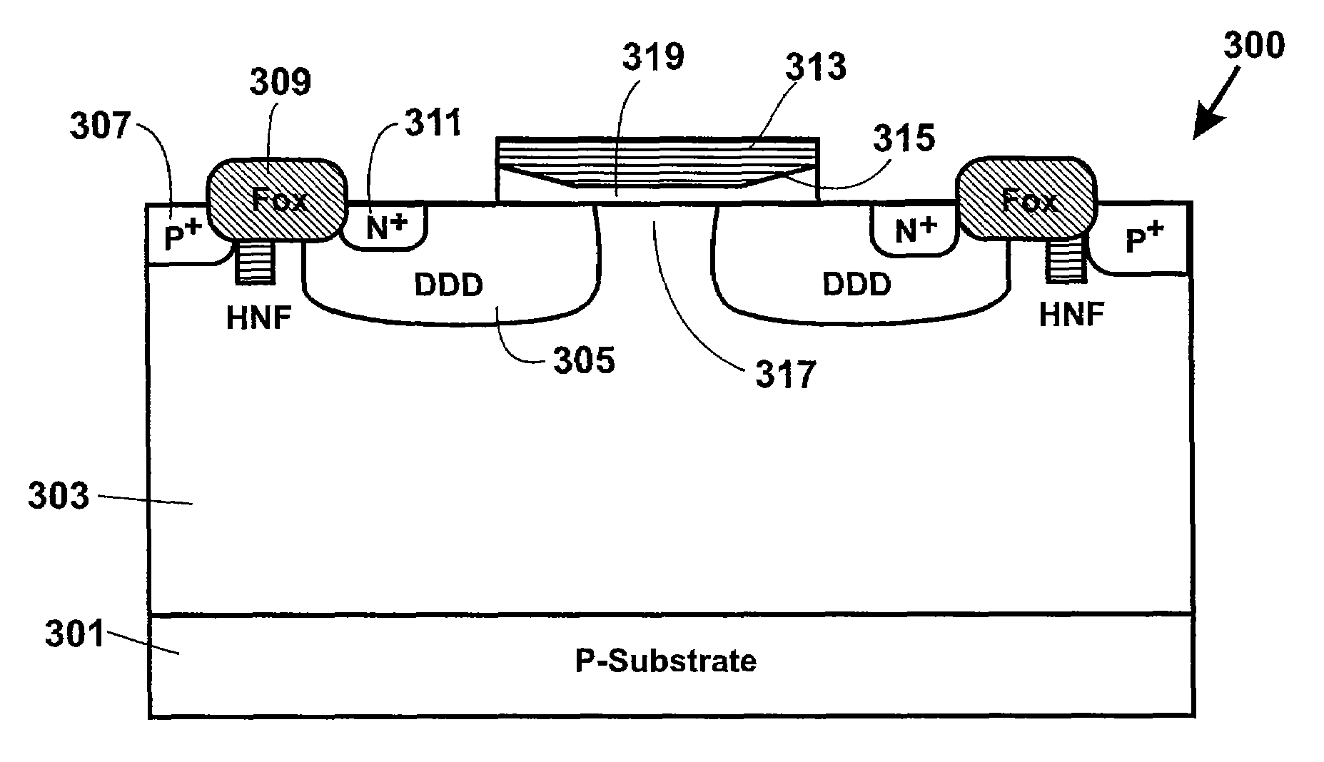
[0015]According to the present invention, techniques for processing integrated circuits for the manufacture of semiconductor devices are provided. More particularly, the invention provides a method for manufacturing a high voltage MOS transistor switching device. But it would be recognized that the invention has a much broader range of applicability.

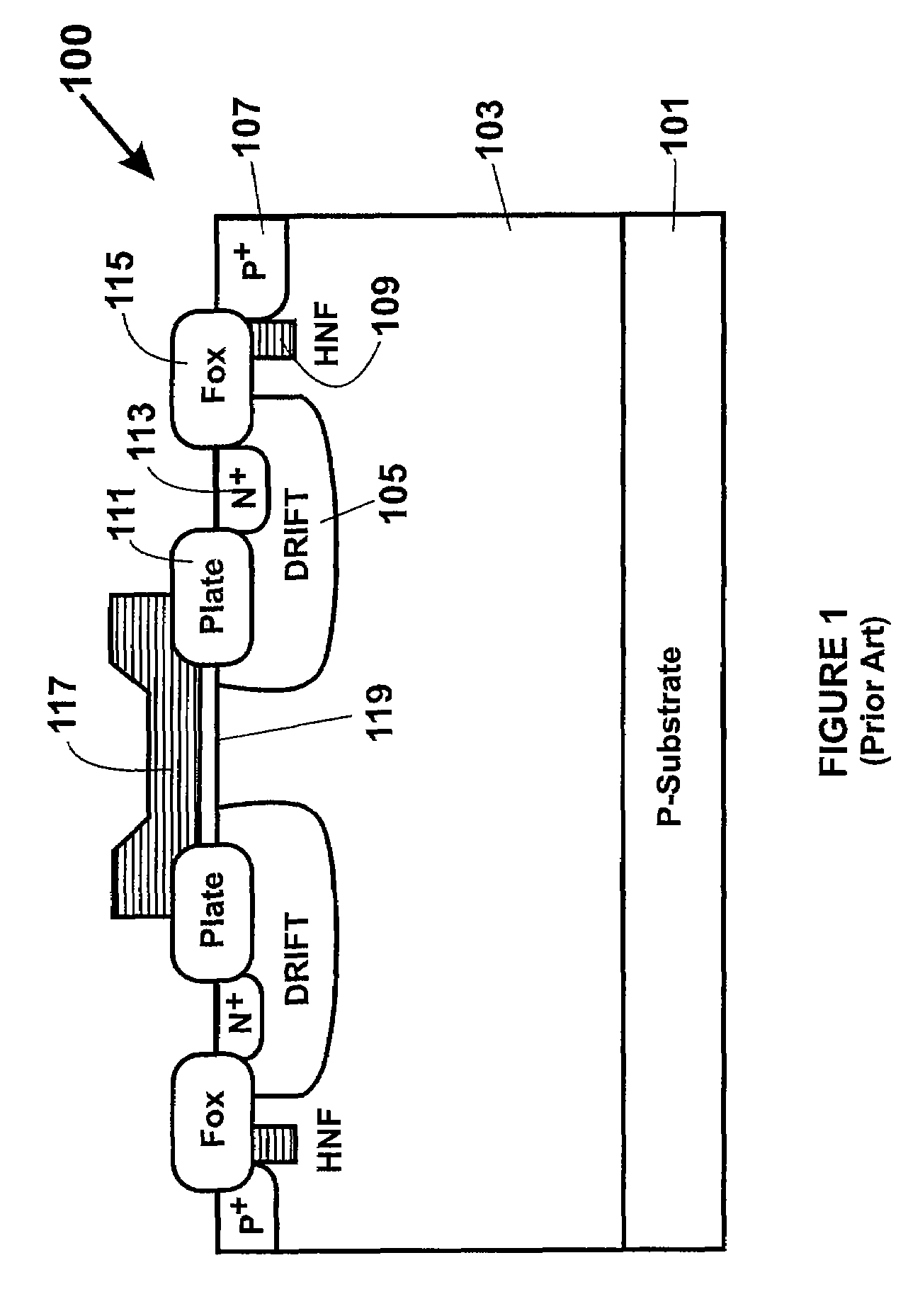
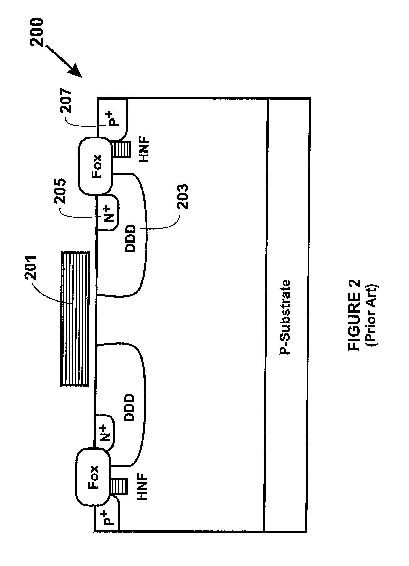
[0016]Before discussing details of the present invention, we have provided a brief description of certain limitations of conventional high voltage MOS devices, which we have uncovered. MOS transistors characterized by more than 30V operation generally use Lateral Drain Device MOS structures (LDMOS) for higher junction breakdown voltages. Such higher breakdown voltages, unfortunately, comes at the expense of larger device design rules, which will be described in more detail below. MOS transistors that use Extended Drain Diffusion Device MOS structures (DDDMOS) often only operate at around 12V-20V with using smaller device design rules tha...


PUM


Abstract

A high voltage semiconductor device. The high voltage device has a substrate (e.g., silicon wafer) having a surface region. The substrate has a well region within the substrate and a double diffused drain region within the well region. A gate dielectric layer is overlying the surface region. A gate polysilicon layer is overlying the gate dielectric layer. A mask layer is overlying the gate polysilicon layer. The device also has a gate electrode formed within the gate polysilicon layer. The gate electrode has a first predetermined width and a first predetermined thickness. Preferably, the gate electrode has a first side and a second side formed between the first predetermined width. The gate electrode is coupled to the double diffused drain region within the well region. Preferably, the first side has a lower corner overlying the gate dielectric layer and an upper corner underlying the mask layer and the second side has a lower corner overlying the gate dielectric layer and an upper corner underlying the mask layer. A first insulating region formed from polysilicon is formed at the lower corner on the first side of the gate electrode. The first insulating region extends from the first side toward a first preselect region within the gate electrode. A second insulating region formed from polysilicon material is at the lower corner on the second side of the gate electrode. The second insulating region extends from the second side toward a second preselected region within the gate electrode. A second predetermined width is formed between the first preselect region and the second preselected region. The second predetermined width comprises substantially polysilicon material. Preferably, the high voltage device has a breakdown voltage of the high voltage semiconductor device is characterized by a voltage of greater than 20 volts.

Description

CROSS-REFERENCES TO RELATED APPLICATIONS[0001]This application claims priority to Chinese Patent Application No. 200410025738.X, filed on Jun. 28, 2004, and is incorporated herein by reference.BACKGROUND OF THE INVENTION[0002]The present invention is directed to integrated circuits and their processing for the manufacture of semiconductor devices. More particularly, the invention provides a method for manufacturing a high voltage MOS transistor switching device. But it would be recognized that the invention has a much broader range of applicability.[0003]Integrated circuits have evolved from a handful of interconnected devices fabricated on a single chip of silicon to millions of devices. Conventional integrated circuits provide performance and complexity far beyond what was originally imagined. In order to achieve improvements in complexity and circuit density (i.e., the number of devices capable of being packed onto a given chip area), the size of the smallest device feature, also...

Claims


Application Information

Patent Timeline
Patent Type & Authority Patents(United States)
IPC IPC(8): H01L21/336H01L29/423H01L29/78
CPCH01L29/42368H01L29/6659H01L29/7836
Inventor CHEN, JOHNLEE, ROGER
Owner SEMICON MFG INT (SHANGHAI) CORP
Why Eureka
Try Eureka