

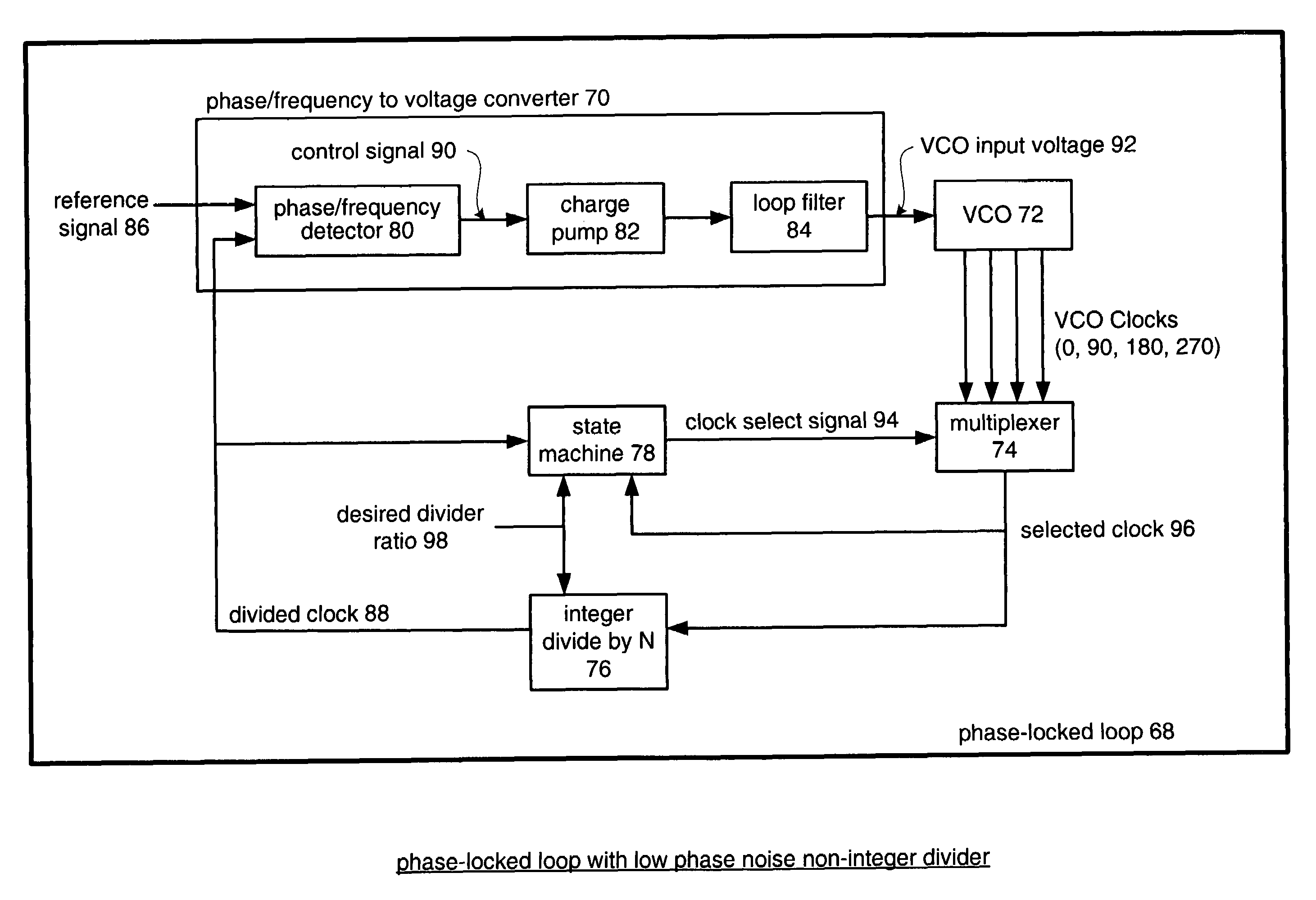
PLL with low phase noise non-integer divider
a phase noise non-integer and phase noise technology, applied in the field of communication systems, can solve the problems of limiting the usefulness of prior art clock recovery circuits, reducing the clock recovery rate of high-speed circuits, and limiting the bandwidth of prior art designs, so as to achieve the effect of expanding and contracting
- Summary
- Abstract
- Description
- Claims
- Application Information
AI Technical Summary
Benefits of technology
Problems solved by technology
Method used
Image

Examples
Embodiment Construction
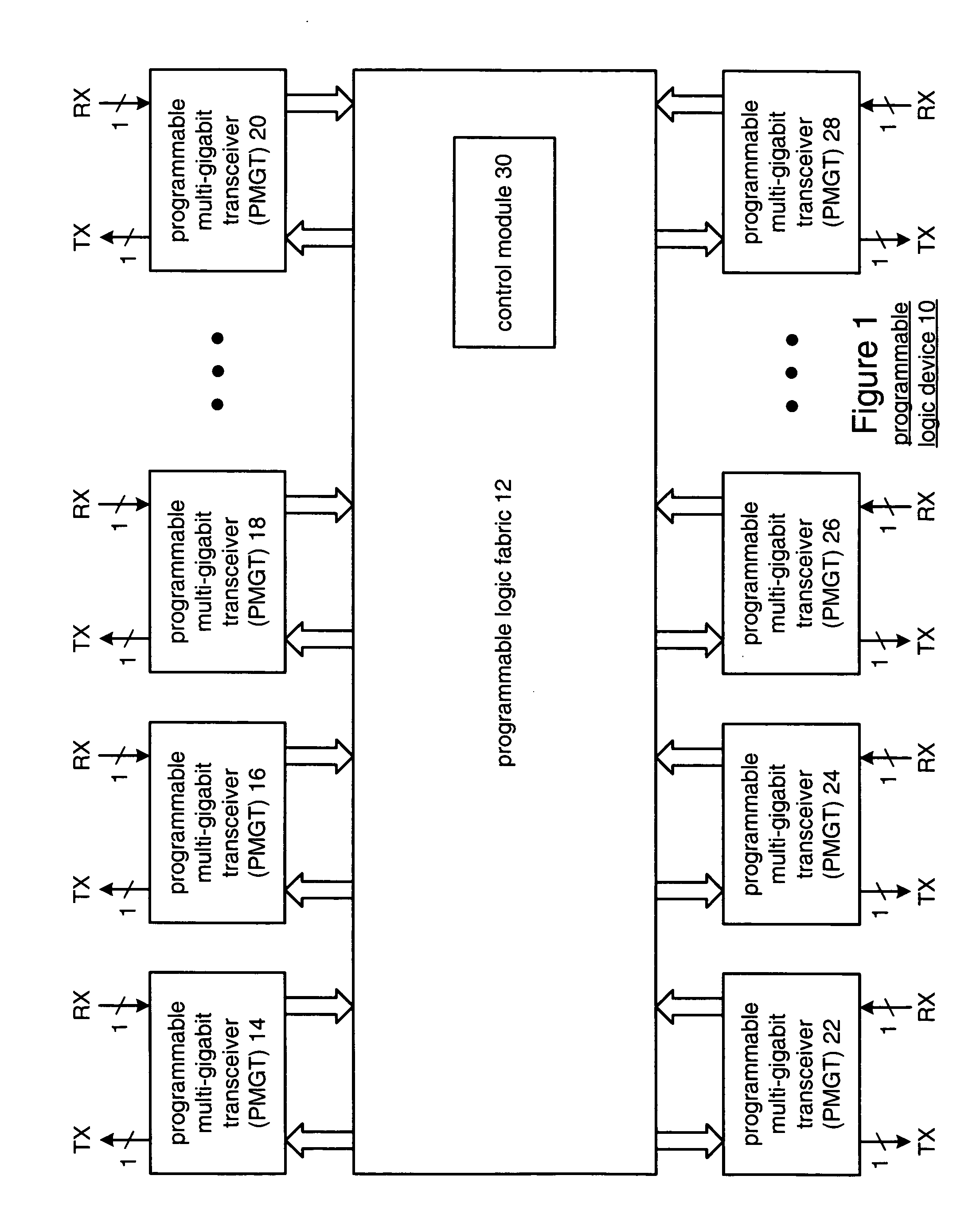
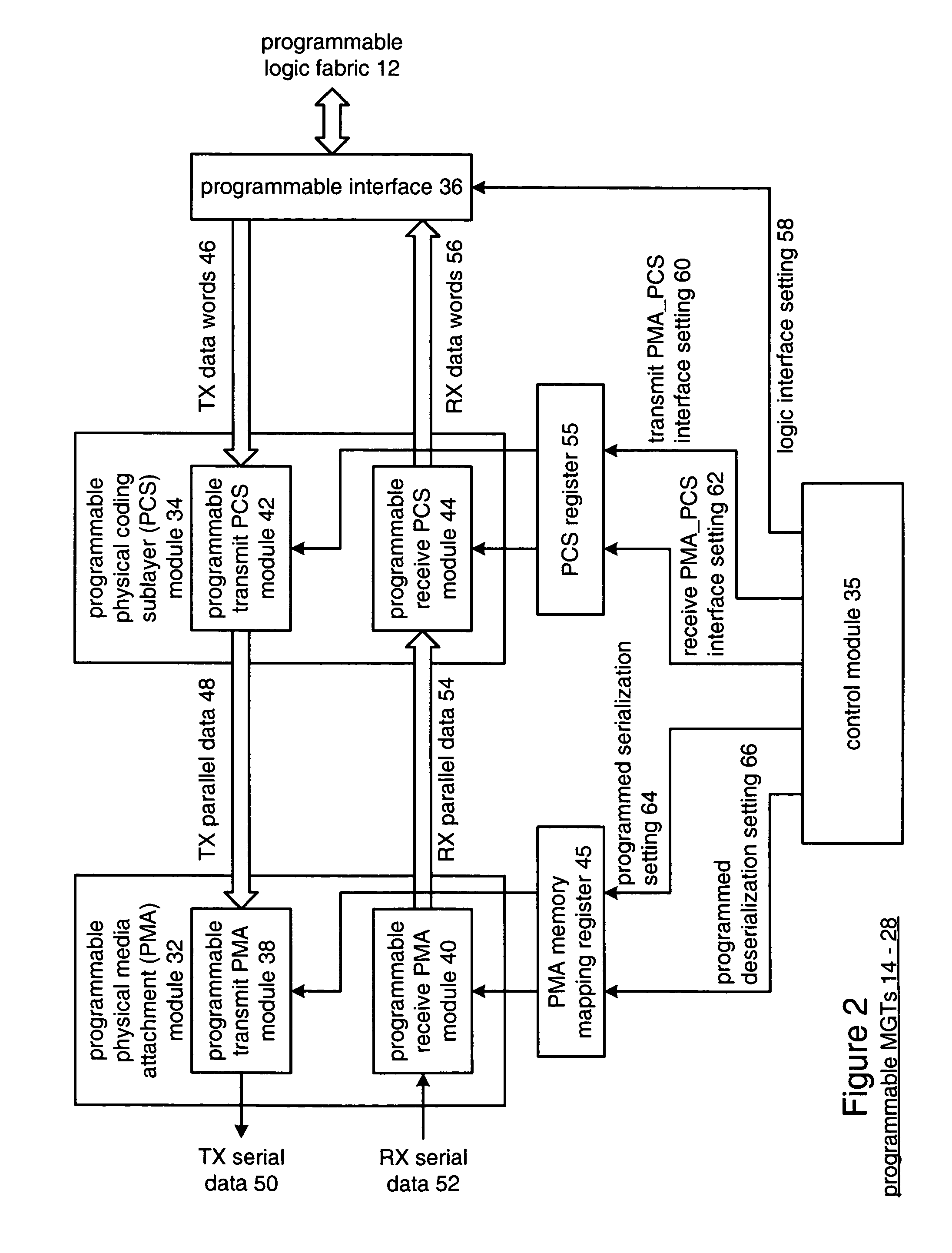
[0025]FIG. 1 is a schematic block diagram of a programmable logic device 10 that includes programmable logic fabric 12, a plurality of programmable multi-gigabit transceivers (PMGTs) 14-28 and a control module 30. The programmable logic device 10 may be a programmable logic array device, a programmable array logic device, an erasable programmable logic device, and / or a field programmable gate array (FPGA). When the programmable logic device 10 comprises a FPGA, the programmable logic fabric 12 may be implemented as a symmetric array configuration, a row-based configuration, a sea-of-gates configuration, and / or a hierarchical programmable logic device configuration. The programmable logic fabric 12 may further include at least one dedicated fixed processor, such as a microprocessor core, to further facilitate the programmable flexibility offered by programmable logic device 10.
[0026]The control module 30 may be contained within the programmable logic fabric 12 or it may be a separate...
PUM
 Abstract
Description
Claims
Application Information