Integration of a waveguide self-electrooptic effect device and a vertically coupled interconnect waveguide

Active Publication Date: 2008-02-26
NAT TECH & ENG SOLUTIONS OF SANDIA LLC
View PDF6 Cites 1 Cited by
  • Summary
  • Abstract
  • Description
  • Claims
  • Application Information

AI Technical Summary

Benefits of technology

[0014]In one variation, light is laterally confined in the waveguide by a rib layer, which also serves as a spacer layer between the core of the waveguide and the active waveguide layer of the SEED. The SEED itself is fabricated as a mesa, with the spacer layer, active waveguide layer and top cladding layer all being part of the mesa. In addition, trenches on both sides of the SEED mesa further can serve to laterally confine the propagating light within the SEED. The length of the trenches preferably is chosen to reduce reflections and decrease associated loss.

Problems solved by technology

In these proposed circuits, SEEDs typically implement the logic functions and the SEEDs are optically interconnected by some means, thus forming a potentially complex logic circuit.
Regardless of the selected approach, the basic geometry of surface-normal SEEDs complicates the interconnection task due to the out-of-plane aspect.
However, the in-plane interconnection of waveguide SEEDs faces other challenges.
However, since regrowth involves the complete removal of the active material and its replacement with new material, the complexity of this method leads to a low yield of functional circuits and a corresponding increase in cost per circuit.
This problem is compounded as the complexity of circuits increases, thus limiting the scalability of this approach.
However, disordering does not allow for removal of doping species or for the reconfiguration of the waveguide.
The impurity doping required to electrically bias the SEED typically causes increased absorptive losses of light propagation in the waveguide.
In the case of even moderately complex optical circuits, these losses can quickly reach a level where little usable light remains in the circuit.
Similarly, layered structures designed as SEEDs are generally not ideal waveguides for propagation of light in a circuit.

Method used


Image

  • Integration of a waveguide self-electrooptic effect device and a vertically coupled interconnect waveguide
  • Integration of a waveguide self-electrooptic effect device and a vertically coupled interconnect waveguide
  • Integration of a waveguide self-electrooptic effect device and a vertically coupled interconnect waveguide

Examples


Embodiment Construction

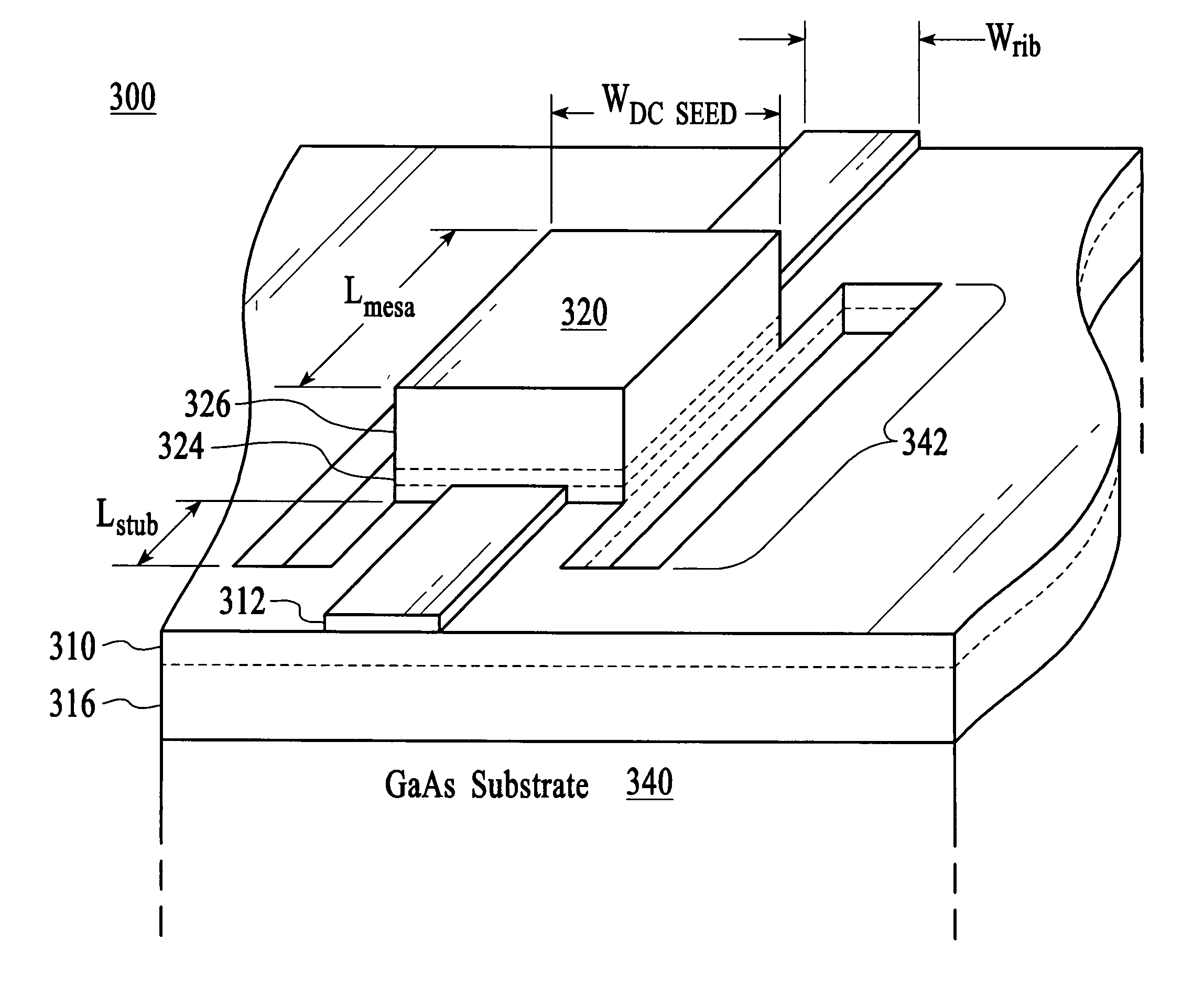
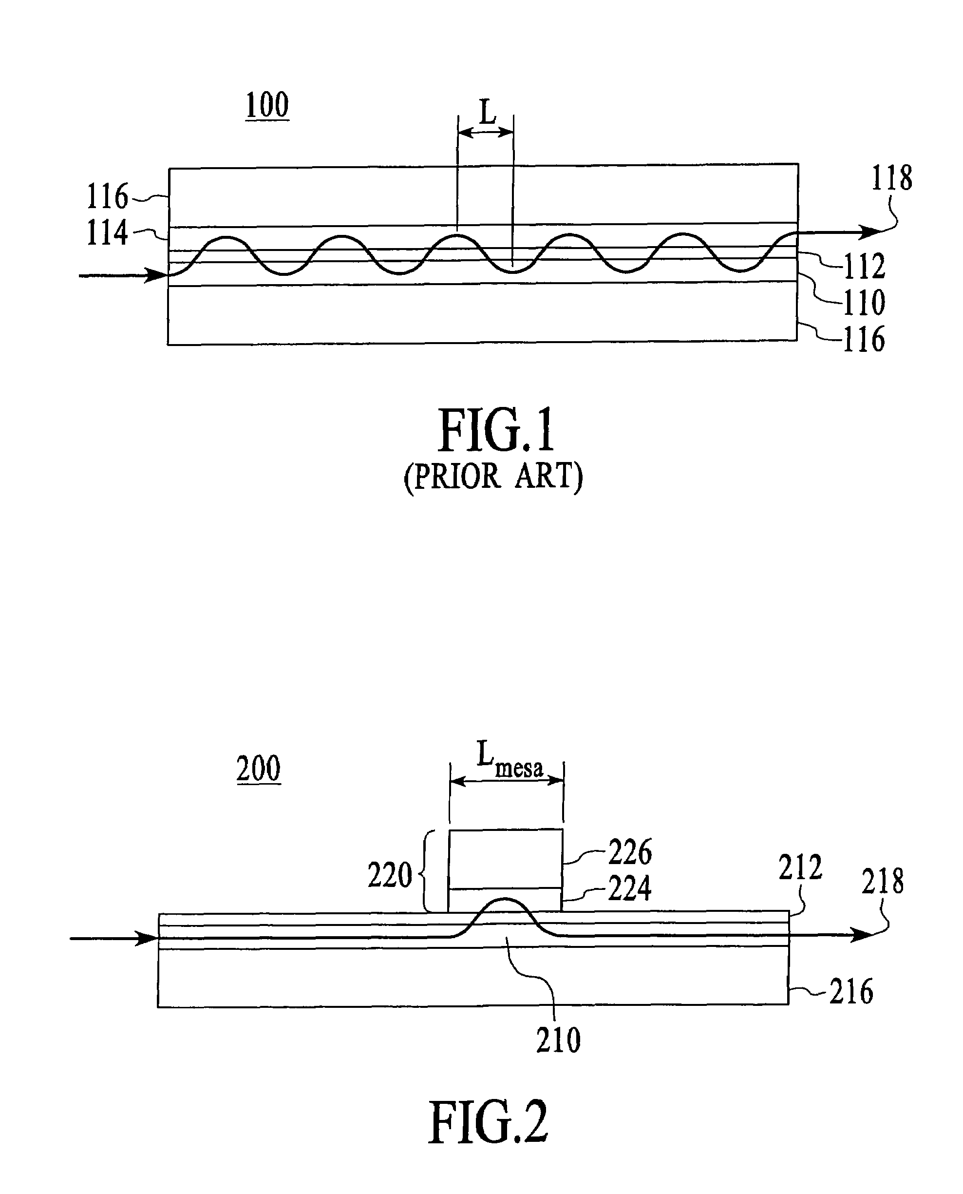
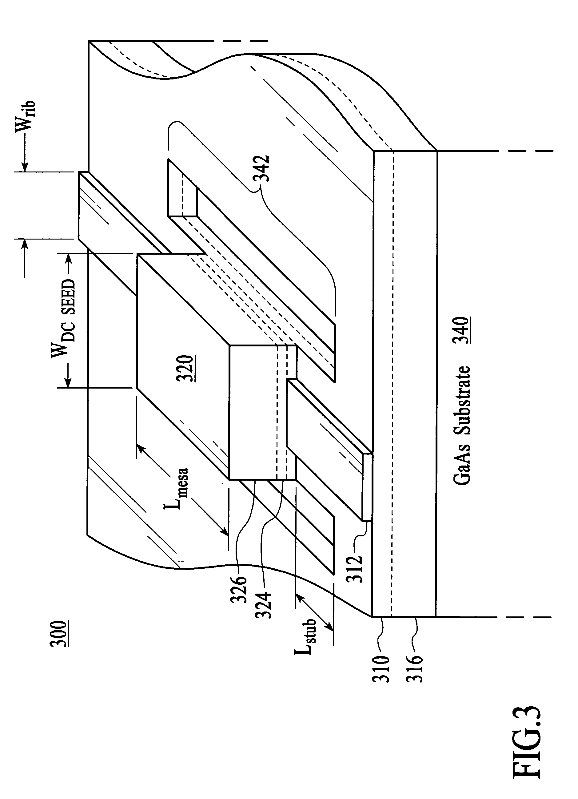
[0025]The SEED circuits described herein use the concept of a vertical directional coupler. The principles of vertical directional couplers have been described, for example, by K. Shimomura and S. Arai in “Semiconductor waveguide optical switches and modulators,” Fiber and Integrated Optics, vol. 13, no. 1, pp. 65-100, January 1994, and Shakouri, Liu et al. in “Wafer-fused Optoelectronics for Switching,” Journal of Lightwave Technology, vol. 16, no. 12, pp. 2236-2242, December 1998. Two optical waveguides having similar modal effective refractive indices are positioned atop one another with a spacer layer of waveguide cladding material separating the two guide layers. The device obeys the well-known principal of evanescent coupling of optical power between two similar single-mode optical waveguides.

[0026]FIG. 1 illustrates the principle of evanescent coupling of optical power between two waveguides 110, 114 in a vertical directional coupler 100. In FIG. 1, two single-mode waveguides...


PUM


Abstract

A self-electrooptic effect device (“SEED”) is integrated with waveguide interconnects through the use of vertical directional couplers. Light initially propagating in the interconnect waveguide is vertically coupled to the active waveguide layer of the SEED and, if the SEED is in the transparent state, the light is coupled back to the interconnect waveguide.

Description

GOVERNMENT RIGHTS STATEMENT[0001]This invention was developed under Contract DE-AC04-94AL85000 between Sandia Corporation and the U.S. Department of Energy. The U.S. Government has certain rights in this invention.BACKGROUND[0002]1. Field of Invention[0003]This invention relates generally to self-electrooptic effect devices and, more particularly, to the integration of waveguide self-electrooptic effect devices with other waveguides.[0004]2. Description of the Related Art[0005]Self-electrooptic effect devices (“SEEDs”) are optoelectronic devices that exhibit optical bistability based on the intensity of incident light. The operation of a SEED using multiple quantum well (“MQW”) material has been well described, for example, by D. A. B. Miller et al. in “Novel hybrid optically bistable switch: The quantum well self-electro-optic effect device,” Appl. Phys. Lett. 45 (1), 1 Jul. 1984. SEEDs have received attention because of their potential for use as components of optical logic circui...

Claims


Application Information

Patent Timeline
IPC IPC(8): G02B6/42
CPCB82Y20/00G02F1/01708G02F3/028
Inventor VAWTER, G. ALLEN
Owner NAT TECH & ENG SOLUTIONS OF SANDIA LLC
Why Eureka
Try Eureka