Structured ASIC device with configurable die size and selectable embedded functions

a technology of asic devices and die sizes, applied in the direction of instruments, semiconductor/solid-state device details, pulse techniques, etc., can solve the problems of increasing the development cost limiting the use of cell-based and hand-crafted custom ic's to very high-volume cost-sensitive applications, and reducing the number of base wafer designs. , the effect of reducing the cost of tooling

Active Publication Date: 2008-02-26
SEMICON COMPONENTS IND LLC
View PDF27 Cites 225 Cited by
  • Summary
  • Abstract
  • Description
  • Claims
  • Application Information

AI Technical Summary

Benefits of technology

[0020]The principles of the present invention are directed towards reducing the number of base wafer designs and reducing tooling costs associated with design and fabrication of Application Specific Integrated Circuit (ASIC) devices. One embodiment provides for a master or universal base and base tooling which addresses the general purpose Structured ASIC requirements. Another embodiment provides for a common set of base tooling from which the master / universal base is created as well as additional custom bases with customized selection and quantity of embedded Platform ASIC functions. Embodiments can utilize conventional Structured ASIC architecture and processing and are compatible with traditional wafer probing and packaging methods and technologies.

Problems solved by technology

However, gate arrays often lack the flexibility to support more complex functionality such as, for example, large amounts of memory, timing generator functions and other specialized functions (e.g., processors and I / O physical interfaces).
Unfortunately, with advances in process technology, the resulting development cost of cell-based and hand-crafted custom IC's is rising exponentially, due at least in part to the cost of photolithographic reticle tooling.
This increased development cost essentially limits the use of cell-based and hand-crafted custom IC's to very high-volume cost-sensitive applications.
That is, it may be difficult to implement high-complexity low-volume applications in a cost efficient manner.
One challenge in selecting the architecture of structured ASIC devices is deciding what type of and in what quantity pre-designed functional blocks should be embedded in the base.
If the appropriate IP functions are not included, the corresponding device will not be usable for certain applications.
If too many embedded IP functions are unused in a particular application, significant silicon area will be unused, potentially making the cost of the device too high.
However, developing multiple platforms each requiring a number of bases (e.g., 6 to 12) requires a significant financial investment.
Further, there are other tooling costs in addition to the photolithographic reticles discussed above.
Each base in a Structured (or Platform) ASIC family will require these additional types of tooling, and thus, will incur some additional corresponding cost, which can usually be distributed across multiple custom logic devices.
However, the borderless approach faces several problems.
One problem is finding an effective way to achieve isolation from the scribe line region.
Scribe lines defined in the programmable levels may provide good definition of the cutting region but since scribe lines typically do not extend into base layers, good isolation is difficult to achieve.
A second problem arises due to the intrinsic differences between transistors designed for use in core logic functions and those intended for use in I / O functions.
Various approaches have been used to achieve dual-use transistors, but the disparity in core and I / O transistor requirements continues to widen, making it evermore difficult to create efficient dual-use structures.
Most borderless approaches do not handle alignment marks and other photolithograhic and processing artifacts very efficiently, often resulting in significant wasted silicon real estate.
Accordingly, it may be difficult to align repeating patterns on the base with repeating patterns on programmable levels.
Many existing mechanisms avoid this alignment issue by intentionally wasting space.
As such they are typically directed to prototyping and are typically not useful for volume production.
However, one-dimensional bordered arrays require that I / O functions are restricted to running along the two side borders.
Thus, problems with isolation in the scribe line regions in the unbordered direction and problems with repeating patterns of alignment and other manufacturing artifacts still exist.
However, these two-dimensional bordered arrays have been limited to the traditional sea-of-transistor architecture.
However, problems related to isolating circuitry in the scribe line regions and dealing with the multitude of alignment, manufacturing and testing artifacts placed on a wafer surrounding the individual die still exist.
These problems are particularly acute when the base die reticle fields have a different repeat sequence than the programmable level reticle fields.

Method used


Image

  • Structured ASIC device with configurable die size and selectable embedded functions
  • Structured ASIC device with configurable die size and selectable embedded functions
  • Structured ASIC device with configurable die size and selectable embedded functions

Examples


Embodiment Construction

[0040]The principles of the present invention are directed towards reducing the number of base wafer designs and reducing base tooling expenses associated with structured and platform ASICs while optimizing die size for individual applications.

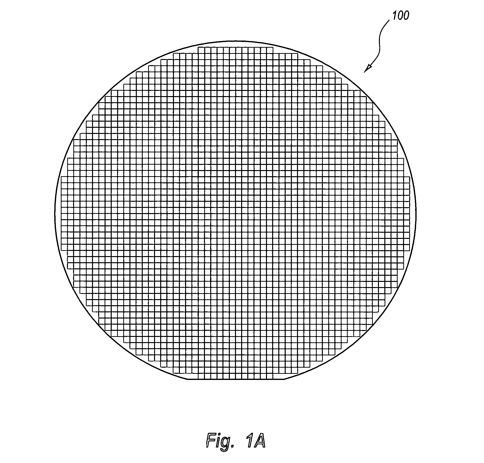
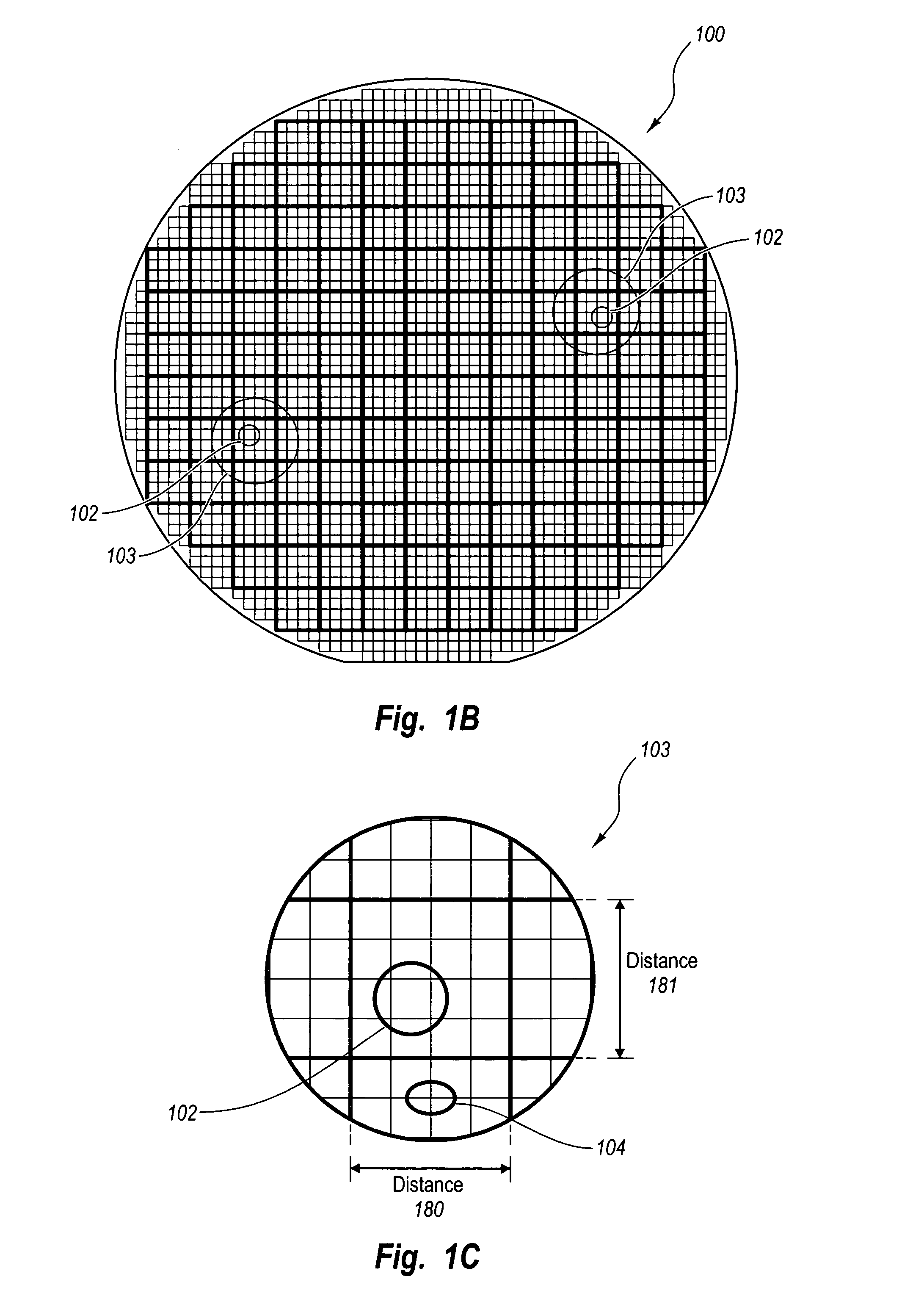
[0041]Generally, silicon wafers used in the fabrication of integrated circuits can be partially fabricated up through a desired processing level (e.g., to implement partial IC functionality). The wafer at this stage is commonly referred to as a “base wafer”. To accomplish this, one or more levels are created through a conventional photolithographic process involving a series of printing and processing steps. For each level, a pattern is printed on a reticle with appropriate alignment marks for aligning of the reticle to the previous levels on the base wafer. The pattern of the reticle is applied to the surface of the base wafer to print a pattern on a portion of the wafer. Then, the reticle is stepped to other locations on the wafer using the ...


PUM


Abstract

One embodiment of the present invention provides for a master or universal base and base tooling which addresses the general purpose Structured ASIC requirements. Another embodiment of the present invention provides for a common set of base tooling from which the master / universal base is created as well as additional custom bases with customized selection and quantity of embedded Platform ASIC functions. Embodiments can utilize conventional Structured ASIC architecture and processing and are compatible with traditional probing and packaging.

Description

BACKGROUND OF THE INVENTION[0001]1. The Field of the Invention[0002]The present invention relates to the field of Application Specific Integrated Circuit (ASIC) design and tooling. In particular, the present invention relates to systems and methods for reducing the number of base wafer designs and reducing tooling costs associated with design and fabrication of structured and platform ASIC devices.[0003]2. Background and Related Art[0004]Various approaches are used to build custom logic Integrated Circuit (“IC”) devices. Different components, such as, for example, prefabricated Programmable Logic Devices (“PLDs”) (sometimes referred to as Field Programmable Gate Arrays (“FPGAs”)), gate arrays, standard cells (sometimes referred to as cell-based ICs), and hand-crafted custom logic, can be used to implement a custom logic IC device. Each of the different components is associated with a number of design parameters, such as, for example, development cost, unit cost, design cycle time, m...

Claims


Application Information

Patent Timeline
Patent Type & Authority Patents(United States)
IPC IPC(8): G06F17/50H01L21/78H01L27/118H03K3/00H03K17/693
CPCH03K17/693G06F2217/64H01L21/78H01L27/11807G03F1/50G06F2115/06
Inventor KIRK, ROBERT S.
Owner SEMICON COMPONENTS IND LLC
Why Eureka
Try Eureka