

Liquid crystal display comprising an electrostatic protection element formed between adjacent bus lines
a liquid crystal display and electrostatic protection technology, applied in non-linear optics, instruments, optics, etc., can solve the problems of not taking static electricity measurement in the process, unable to apply independent signals to each bus line, and reducing the fabrication yield of panels, etc., to achieve gentle static electricity, reduce the load on the first tft, and improve the redundancy of the electrostatic protection circuit
- Summary
- Abstract
- Description
- Claims
- Application Information
AI Technical Summary
Benefits of technology
Problems solved by technology
Method used
Image

Examples
first embodiment
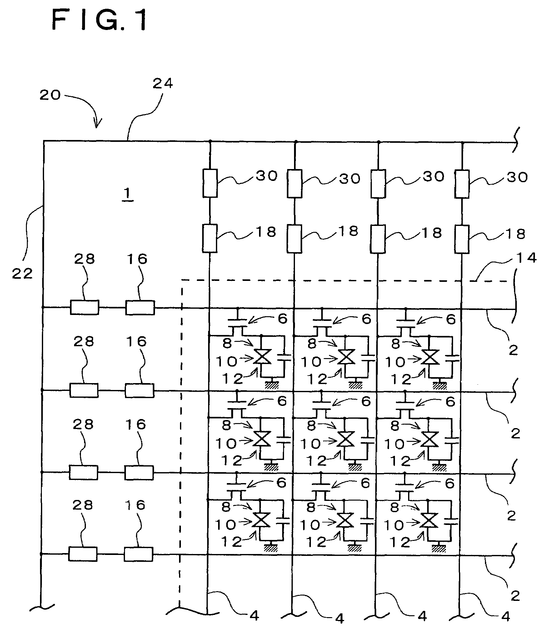
[0076]A liquid crystal display according to the present invention is described with reference to FIG. 1, FIG. 2a and FIG. 2b. First, a schematic structure of the liquid crystal display according to this embodiment is described with reference to FIG. 1. FIG. 1 shows a part of a substrate 1 on an array side of this liquid crystal display viewing toward a substrate surface. It will be noted that inside of a pixel area shows an equivalent circuit for driving liquid crystal. On the substrate 1 on the array side, a plurality of gate bus lines 2 extending in the horizontal direction in the diagram are formed in parallel in the vertical direction. Furthermore, although omitted in the diagram, an insulation film is formed on the plurality of gate bus lines 2, and a plurality of data bus lines 4 are formed on the insulation film in substantially orthogonal to the gate bus lines 2. Each area decided by the gate bus lines 2 and the data bus lines 4 which cross orthogonally to each other in a ma...
second embodiment
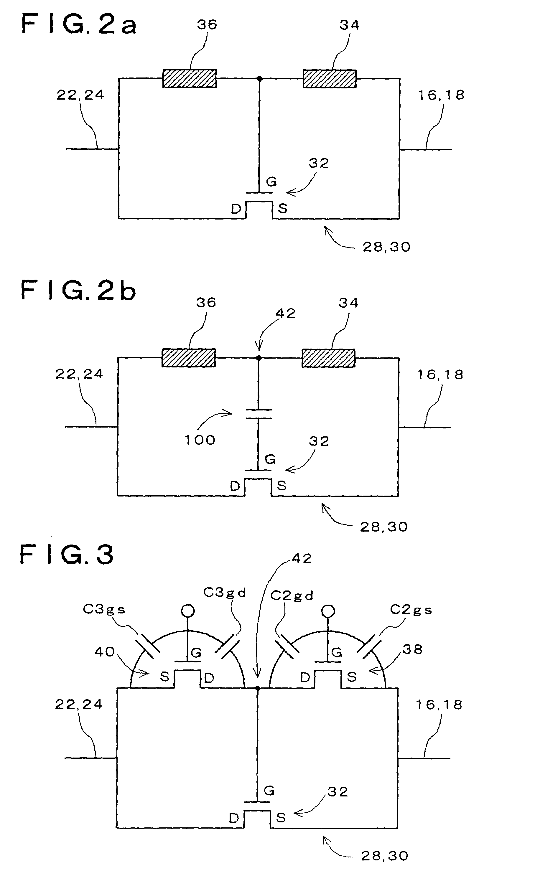
[0118]If the common TFT 41 is used in place of the third TFT 40 in the electrostatic protection element sections 28 and 30 of all the bus lines, the number of structuring elements per a bus line can be approximately 2 and the number of elements used in the electrostatic protection circuits can be reduced to approximately half.
[0119]Next, the structure of the electrostatic protection circuit according to this embodiment is described with reference to FIG. 17. FIG. 17 shows a state of a single electrostatic protection circuit on the substrate 1 on the array side when viewing toward the substrate surface. In FIG. 17, the electrostatic protection element sections 28-1 and 28-n are formed between the common wiring 22 extending vertically in the left side on the diagram and the external output electrodes 16-1 and 16-n.
[0120]In this example, the conductor 42 extends vertically in the diagram and is connected to the gate electrodes of a plurality of the first TFT's 32-1 through 32-n. Furth...
eighth embodiment
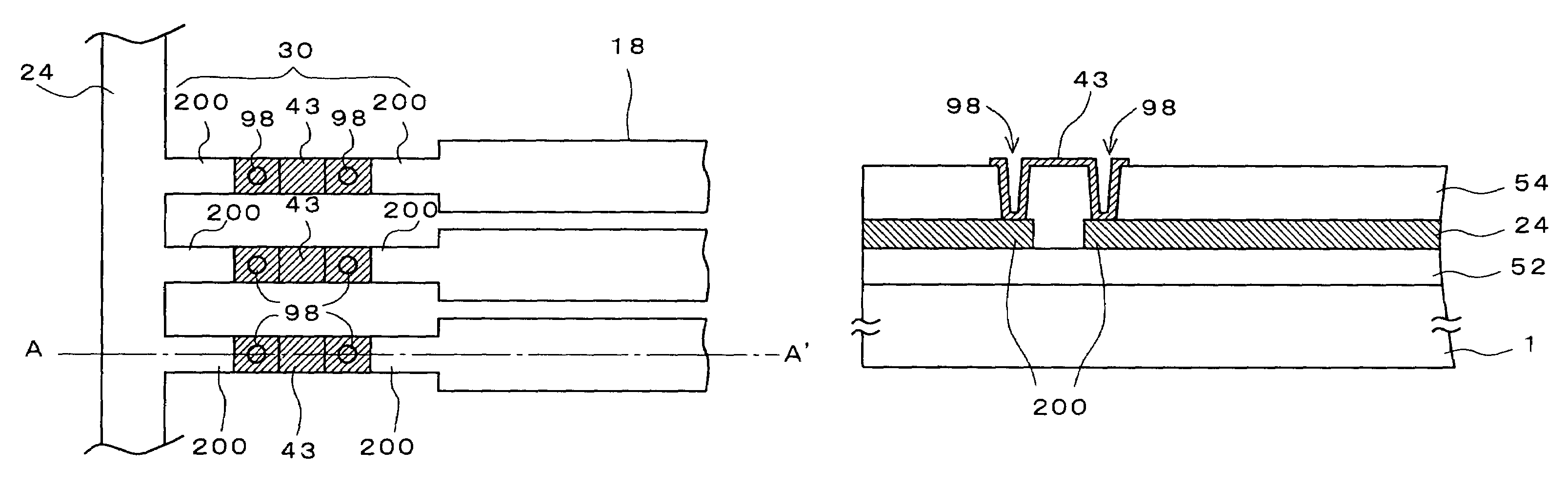
[0128]Next, a liquid crystal display according to the present invention is described. To begin with, a fabrication process of the substrate on the array side for a TFT-LCD used in this embodiment is briefly described. First, a gate metal is deposited and patterned on the substrate on the array side, and the gate bus line and the gate electrode of the TFT in each pixel area are formed. Second, the gate insulation film is formed on the whole surface and an a-Si layer to be an operating semiconductor film of the TFT and an insulation film for forming a channel protection film are deposited in this order on the gate insulation film. Third, by a back exposure using the bus line and the gate electrode as a mask and an exposure using an ordinary mask to electrically separate the a-Si layer from the pixel area, the above insulation film is patterned and the channel protection film is formed. Fourth, an n+ layer to be an ohmic contact layer, the drain / source electrodes and a drain metal (for...
PUM
| Property | Measurement | Unit |
|---|---|---|
| contact resistance | aaaaa | aaaaa |
| resistance | aaaaa | aaaaa |
| resistance | aaaaa | aaaaa |
Abstract
Description
Claims
Application Information