Lens array for electron beam lithography tool

a technology of electron beam lithography and electron beam, which is applied in the direction of beam deviation/focusing by electric/magnetic means, instruments, therapy, etc., can solve the problem that the raster scan mode is too slow to enable the high throughput required in semiconductor wafer processing, and achieve the effect of reducing spherical aberration

Inactive Publication Date: 2008-03-18
LUCENT TECH INC +1
View PDF28 Cites 6 Cited by
  • Summary
  • Abstract
  • Description
  • Claims
  • Application Information

AI Technical Summary

Benefits of technology

[0009]In another embodiment of the present invention, the mesh grid includes multiple (for example, two, three, or more) meshes. In an odd numbered configuration (greater than one), the outward two meshes may have a curved shape; such a lens would enable beam emittance control and also reduce spherical aberration.

Problems solved by technology

These tools have been widely used for high precision tasks, such as lithographic mask making, but the raster scan mode is found to be too slow to enable the high throughput required in semiconductor wafer processing.
A common drawback of both types is that beam emittance depends on actual Wehnelt bias, which couples beam current control with inevitable emittance changes.

Method used


Image

  • Lens array for electron beam lithography tool
  • Lens array for electron beam lithography tool
  • Lens array for electron beam lithography tool

Examples


example 1

[0047]A LaB6 gun of 0.2 mm diameter is used. The cross-over after the gun lens could be 60 μm, thus the emittance increase is a factor of eight using Grid #1 in Table 1.

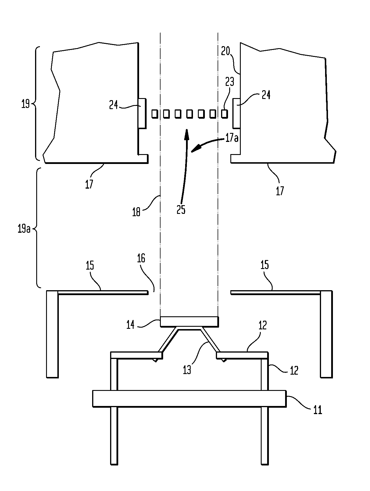
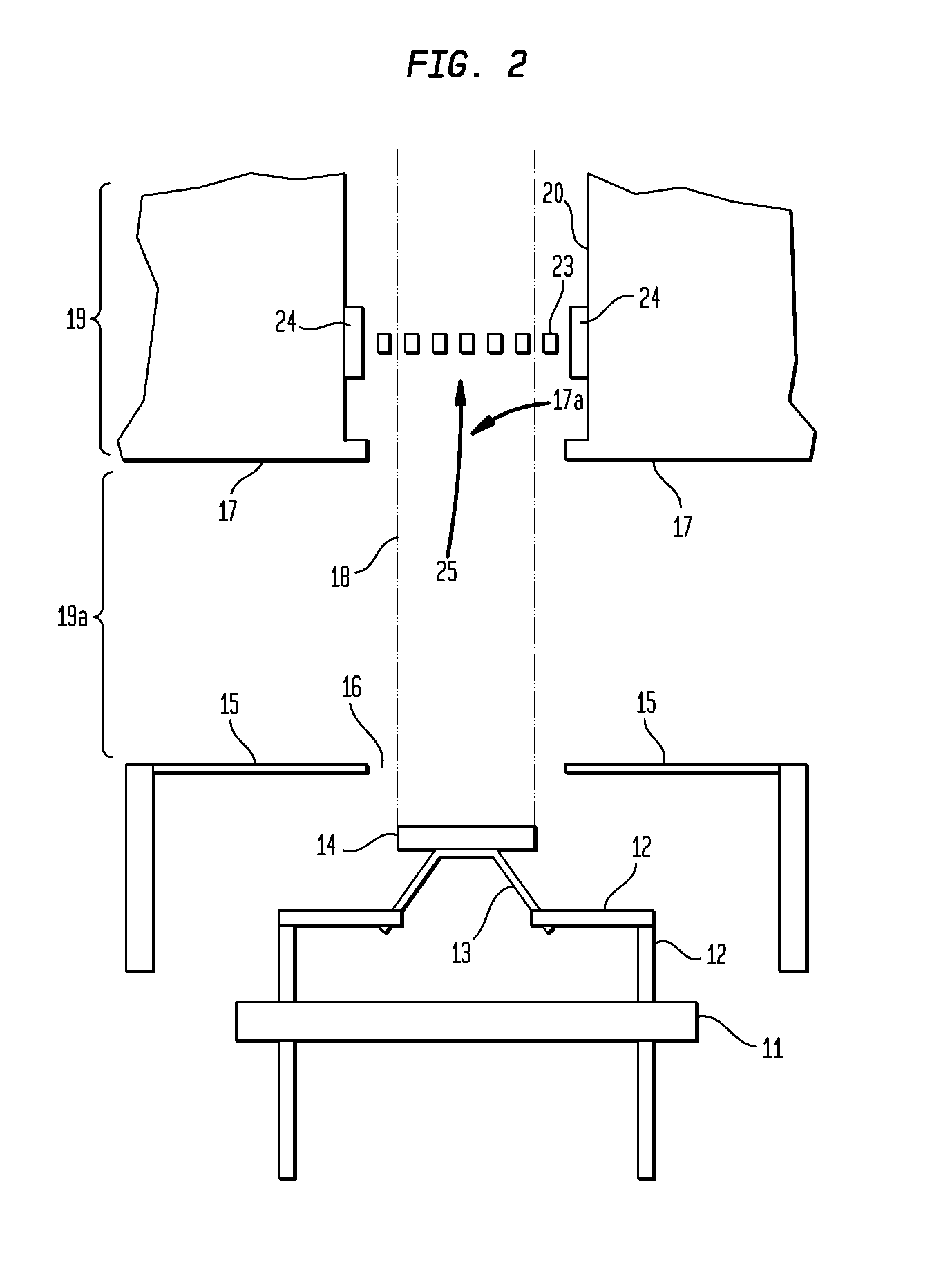
[0048]The lens array 80 may be the mesh grid 23 at potential V1, between liner 20 at potential V0as shown in FIG. 6, or include two grids 23 and 23′ at the potentials illustrated in FIG. 6(a ) or three grids 23, 23′, 23″ at the potentials illustrated in FIGS. 6(b) and 6(c), or any other configuration which contains a grid mesh with an electrostatic field perpendicular to the gridplane.

[0049]The focal distance of the lenslets 85 in FIG. 5 is typically in the order of 4×Vacc / Efield, where Vacc is the acceleration potential of the electron beam and Efield the strength of the electrostatic field. In Example 1, the distance between the gun cross-over and the lens array could be typically 100 mm, calling for a focal length of about 50 mm to create demagnified images. Thus, at 100 kV acceleration, the field should be 10 kV / ...


PUM

PropertyMeasurementUnit
transparencyaaaaaaaaaa
areasaaaaaaaaaa
bias voltageaaaaaaaaaa

Abstract

A method and apparatus for controlling beam emittance by placing a lens array in a drift space of an illumination system component. The illumination system component may be an electron gun or a liner tube or drift tube, attachable to an electron gun. The lens array may be one or more mesh grids or a combination of grids and continuous foils. The lens array forms a multitude of microlenses resembling an optical “fly's eye” lens. The lens array splits an incoming solid electron beam into a multitude of subbeams, such that the outgoing beam emittance is different from the incoming beam emittance, while beam total current remains unchanged. The method and apparatus permit independent control of beam current and beam emittance, which is beneficial in a SCALPEL illumination system.

Description

FIELD OF THE INVENTION[0001]This invention relates to an illumination system for an electron beam lithography apparatus used for the manufacture of semiconductor integrated circuits.BACKGROUND OF THE INVENTION[0002]Electron beam exposure tools have been used for lithography in semiconductor processing for more than two decades. The first e-beam exposure tools were based on the flying spot concept of a highly focused beam, raster scanned over the object plane. The electron beam is modulated as it scans so that the beam itself generates the lithographic pattern. These tools have been widely used for high precision tasks, such as lithographic mask making, but the raster scan mode is found to be too slow to enable the high throughput required in semiconductor wafer processing. The electron source in this equipment is similar to that used in electron microscopes, i.e., a high brightness source focused to a small spot beam.[0003]More recently, a new electron beam exposure tool was develop...

Claims


Application Information

Patent Timeline
Patent Type & Authority Patents(United States)
IPC IPC(8): G21K5/10G21K5/04G03F7/20H01J37/065H01J37/12H01J37/305H01L21/027
CPCH01J37/065H01J37/12H01J2237/1205H01J2237/31774H01L21/027
Inventor KATSAP, VICTORKRUIT, PIETERMOONEN, DANIELWASKIEWICZ, WARREN KAZMIR
Owner LUCENT TECH INC
Why Eureka
Try Eureka