

Semiconductor memory device
a memory device and semiconductor technology, applied in the field of semiconductor memory devices, can solve the problems of inability to perform trimming and large circuit scal
- Summary
- Abstract
- Description
- Claims
- Application Information
AI Technical Summary
Benefits of technology
Problems solved by technology
Method used
Image

Examples
embodiment 1
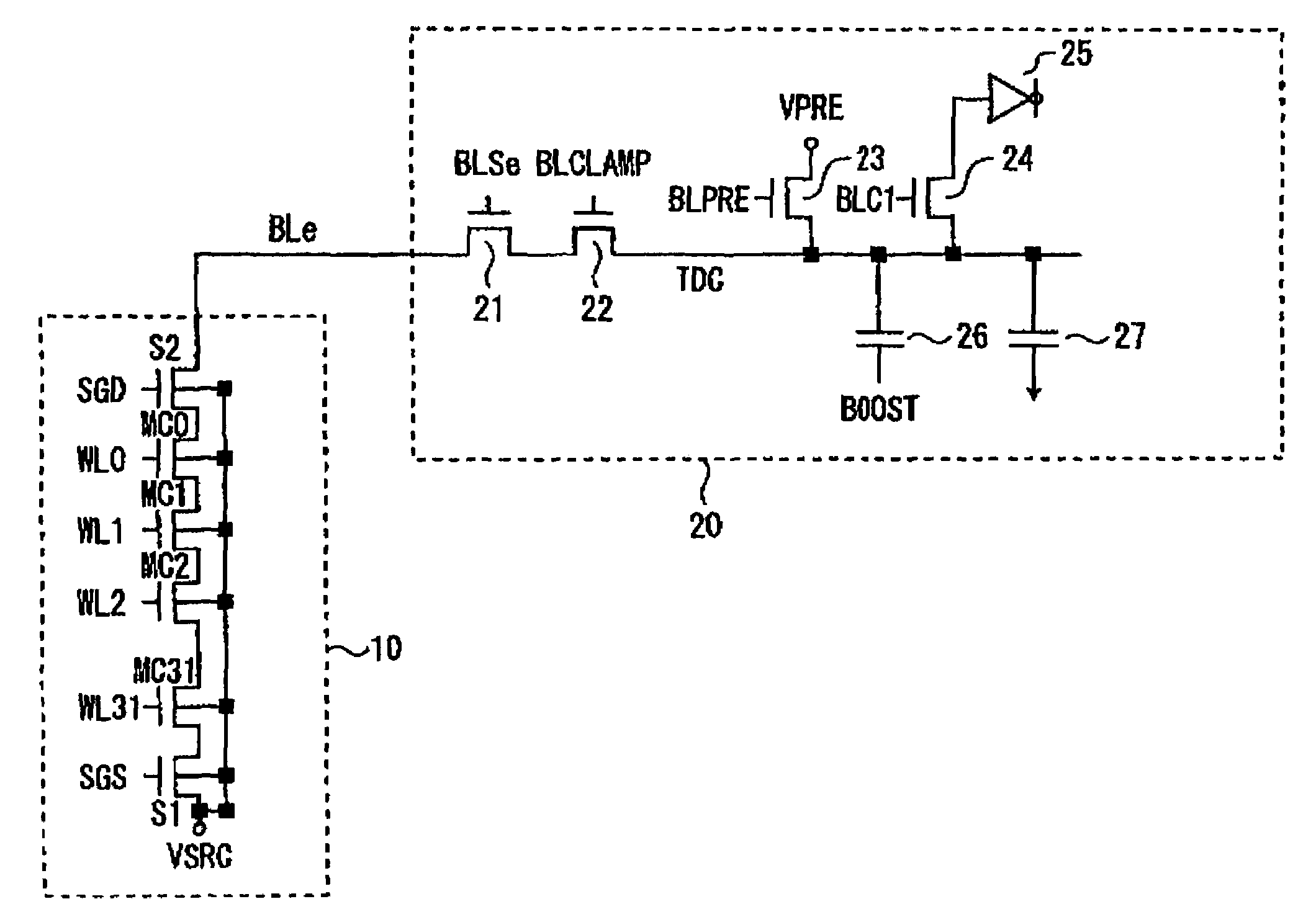
[0023]FIG. 1 is a circuit diagram illustrative of a semiconductor memory device according to an embodiment 1 of the present invention. As shown in FIG. 1, the semiconductor memory device comprises an NAND cell unit 10, and a sense amp circuit 20 connected to a bit line to which the cell unit is connected. In general, an NAND cell array includes a plurality of NAND cell units while FIG. 1 shows only one of the NAND cell units.
[0024]The NAND cell unit 10 includes 32 serially connected memory cells MC0-MC31, and selection gate transistors S1, S2 connected to both ends thereof. The source of the selection gate transistor S1 and the well of the memory cells MC0-MC31 are connected to a common source line (supply line) VSRC, and the drain of the selection gate transistor S2 is connected to a bit line BLe. The control gates of the memory cells MC0-MC31 are connected to respective word lines WL0-WL31, and the gates of the selection gate transistors S1, S2 are connected to selection gate line...
embodiment 2
[0057]FIG. 6 is a circuit diagram illustrative of a semiconductor memory device according to an embodiment 2. In the embodiment 1 one NAND cell unit is described as an example while in this embodiment plural NAND cell units are connected to the sense amp unit. The other same elements as those in FIG. 1 are denoted with the same reference numerals and omitted from the following description. In this embodiment an example equipped with two NAND cell units is described though the number of NAND cell units is not limited to this example.
[0058]As shown in FIG. 6, the sense amp unit 20 has the same arrangement as that in the embodiment 1, which is omitted from the following description. The transistor 22 supplied with the control voltage BLCLAMP in the sense amp unit 20 is branched in accordance with the number of NAND cell units. One branch is connected to the bit line BLe via the transistor 21 having the gate connected to control voltage BLSe. The other is connected to a bit line BLo via...
embodiment 3
[0072]FIGS. 9 and 10 show circuit diagrams of a semiconductor memory device according to an embodiment 3 of the present invention. This embodiment differs from the preceding embodiments in the following. In the preceding embodiments, the voltage on the supply line VSRC and the control voltage BLCLAMP, both temperature characteristic-imparted, are generated using the BGR circuit and so forth. To the contrary, in this embodiment, generation of the temperature characteristic-imparted voltage on the supply line VSRC is left as it is and the temperature characteristic-imparted voltage VSRC is used to generate the control voltage BLCLAMP.
[0073]A voltage generator for the control voltage BLCLAMP is shown in the following circuit diagrams.
[0074]First, as shown in FIG. 9A, the reference voltage VREF and a voltage fed back from a node between a PMOS transistor 61 and a resistor Rz1 are input to a differential amplifier 62. The voltage output from the differential amplifier 62 is fed to the ga...
PUM
 Abstract
Description
Claims
Application Information