Backplateless silicon microphone
a technology of silicon condenser microphone and backplate, which is applied in the direction of transducer details, electrostatic transducer microphones, electrical transducers, etc., can solve the problems of complex fabrication, manufacturing complications, and high cos
- Summary
- Abstract
- Description
- Claims
- Application Information
AI Technical Summary
Benefits of technology
Problems solved by technology
Method used
Image
Examples
first embodiment
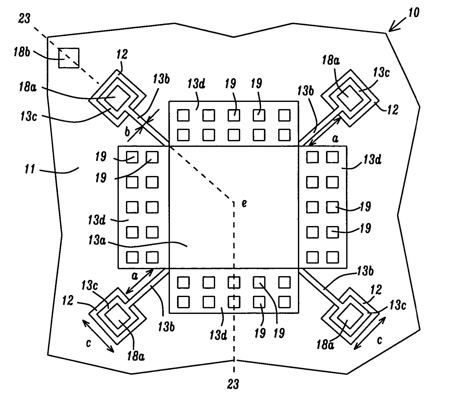
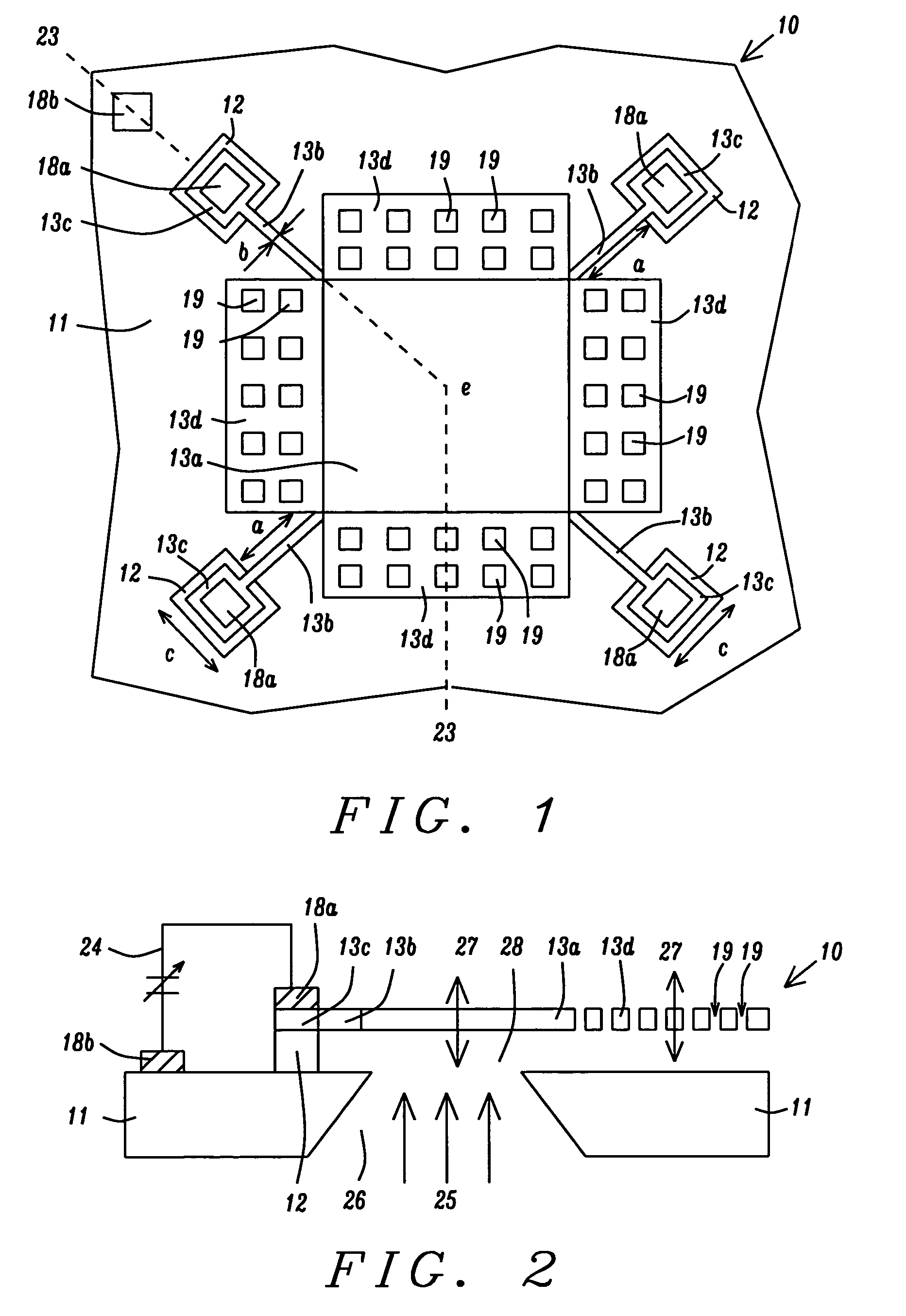
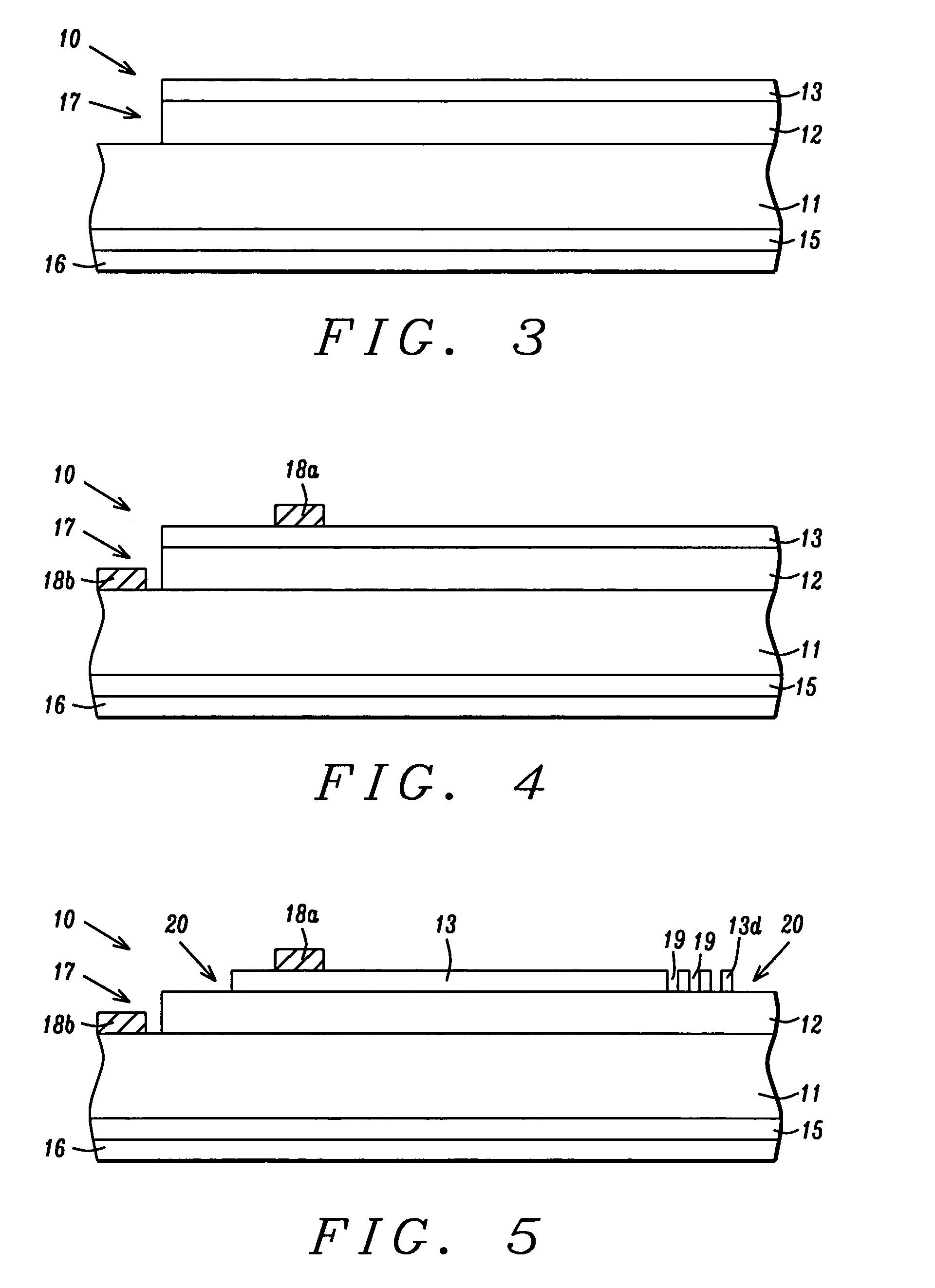
[0028]Referring to FIG. 1, the microphone sensing element according to the present invention is depicted. The microphone sensing element 10 is constructed on a substrate 11 such as silicon which preferably has low resistivity. Optionally, the substrate 11 may be glass with a conductive layer formed thereon. The microphone sensing element 10 is based on a membrane film that is fabricated into diaphragm, mechanical springs, perforated plates, and pads. In the exemplary embodiment, there is an essentially square, planar diaphragm 13a made of silicon, polysilicon that may be doped, Au, Ni, Cu, or other metal materials. Alternatively, the diaphragm may have a rectangular or circular shape. The diaphragm 13a is supported at each of its four corners by mechanical springs 13b which are made of the same material and have the same thickness as the diaphragm. The mechanical springs 13b have a length a, a width b, and are formed along a plane that passes through the diaphragm center e and a cor...
second embodiment
[0033]a sensing element in a backplateless silicon microphone according to the present invention is shown in FIGS. 9-12. The view in FIG. 9 is from a cross-section along the dashed line 47 as illustrated in the top view in FIG. 10. Note that the dashed line 47 is not linear in order to intersect all of the key features in the drawing. Referring to FIG. 9, a microphone sensing element 30 is based on a substrate 31 that is preferably a silicon wafer polished on front and back sides and having a (100) crystal orientation and a 0.01-0.02 ohm-cm resistivity. Optionally, the substrate is comprised of glass with a conductive layer thereon. To reduce the parasitic capacitance, regions on the front side of the substrate 31 that are overlaid by mechanical springs 41c and pads 41d have trenches 32 filled with an oxide layer 33 that also overlays the substrate. The oxide layer 33 and an overlying first polysilicon (poly 1) layer 34 form a stack in the shape of an island that covers the trenches...
third embodiment
[0044]a microphone sensing element according to the present invention is shown in FIGS. 15-18. The view in FIG. 15 is from a cross-section along the dashed line 70 in the top view depicted in FIG. 18. Note that the dashed line 70 is not linear in order to intersect all of the key features in the drawing. Referring to FIG. 15, a microphone sensing element 50 is based on a substrate 51 that is preferably a low resistivity silicon wafer polished on front and back sides. There is a thermal oxide layer 52 disposed on a portion of the front side of substrate 51 and above the thermal oxide layer is an LPCVD silicon nitride layer 53. On an adjacent portion of substrate 51 is a second electrode 63. The second electrode is comprised of a Cr / Au composite layer or is a single layer or composite layer comprised of Al, Ti, Ta, Ni, Cu, or other metal materials.
[0045]The back side of substrate 51 has a stack of layers in which a thermal oxide layer 52b is disposed on the substrate and a silicon nit...
PUM
 Abstract
Description
Claims
Application Information


