Metal gated ultra short MOSFET devices

a technology of metal gate and ultra-short mosfet, which is applied in the field of less than 40 nm gate length field effect devices, can solve the problems of increasing complexity of technology, increasing the risk of affecting the safety of devices, and increasing the difficulty of maintaining performance improvement of devices of deeply submicron generation,

Inactive Publication Date: 2008-03-25
GLOBALFOUNDRIES INC
View PDF9 Cites 123 Cited by
  • Summary
  • Abstract
  • Description
  • Claims
  • Application Information

AI Technical Summary

Problems solved by technology

As FET (Field Effect Transistor) devices are being scaled down, the technology becomes more complex, and changes in device structures and new fabrication methods are needed to maintain the expected performance enhancement from one generation of devices to the next.
There is great difficulty in maintaining performance improvements in devices of deeply submicron generations.
Various detrimental device effects become more serious with successively decreasing device dimensions.
For instance, with shortening gate lengths the so called short channel effects (SCEs), most notably drain-induced barrier lowering (DIBL) pose severe roadblocks to miniaturization.
Many elements needed to support the gate length scaling scheme are approaching physical limitations.
For instance, making junctions highly conductive, and simultaneously of shallow depth, with the use of ion implantation and annealing becomes very difficult, due to dopant activation and diffusion effects.
For standard processes, higher dopant activation (at higher temperatures) is usually accompanied by additional diffusion issues and concerns.
Furthermore, excessive junction leakage may prevent channel doping from being increased beyond the concentration needed to control short channel effects for less than 40 nm gate length devices.

Method used


Image

  • Metal gated ultra short MOSFET devices
  • Metal gated ultra short MOSFET devices
  • Metal gated ultra short MOSFET devices

Examples


Embodiment Construction

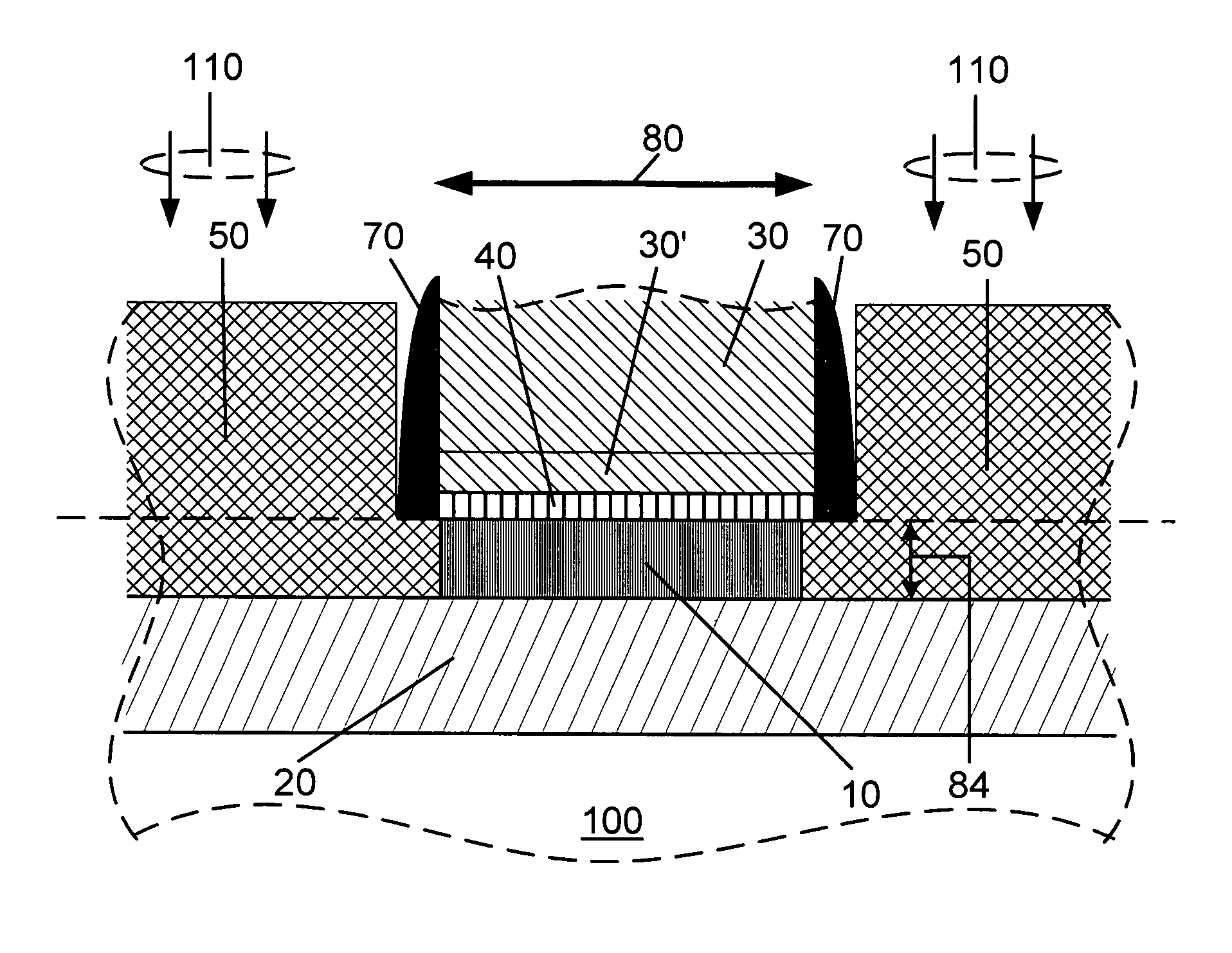
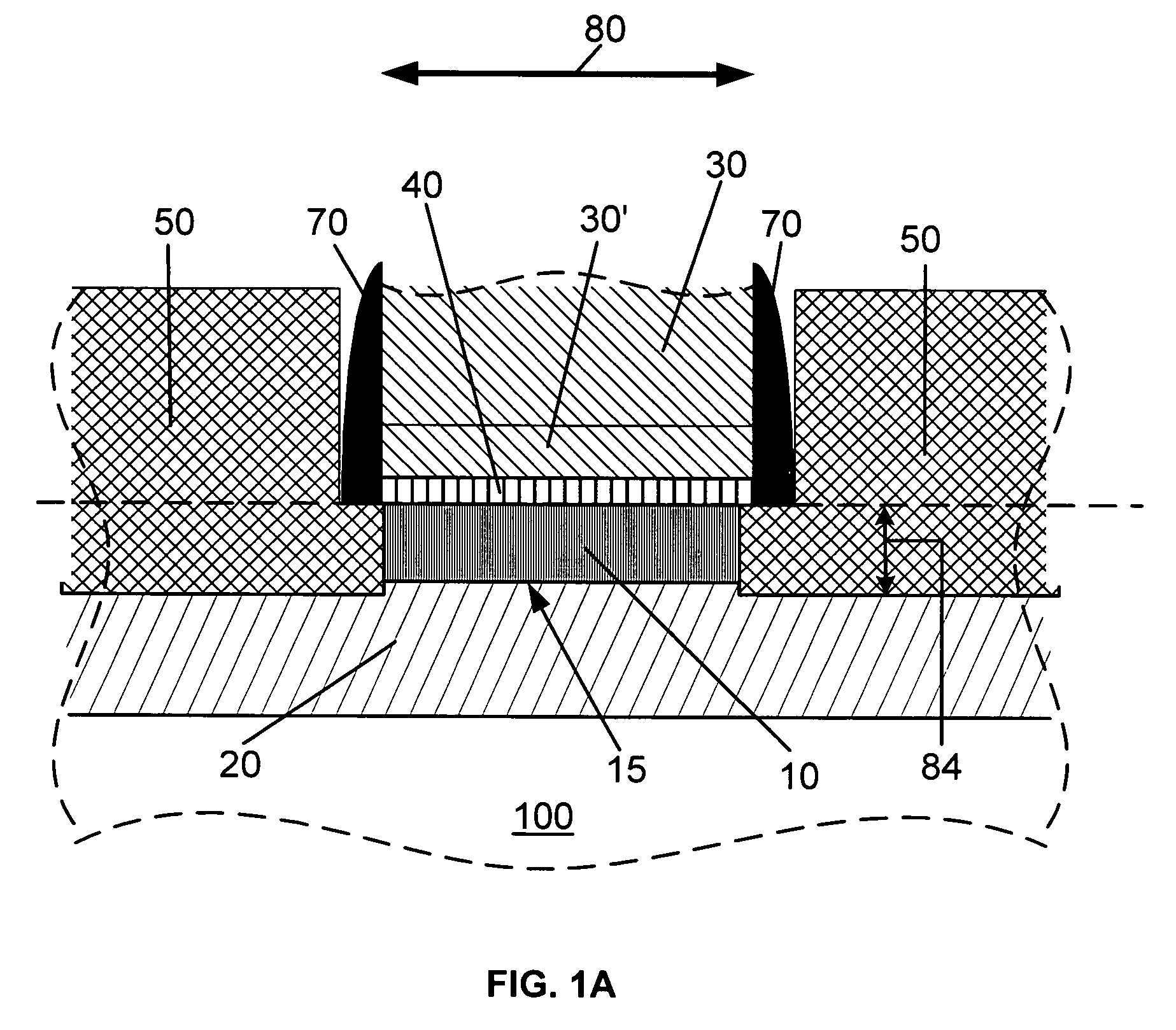
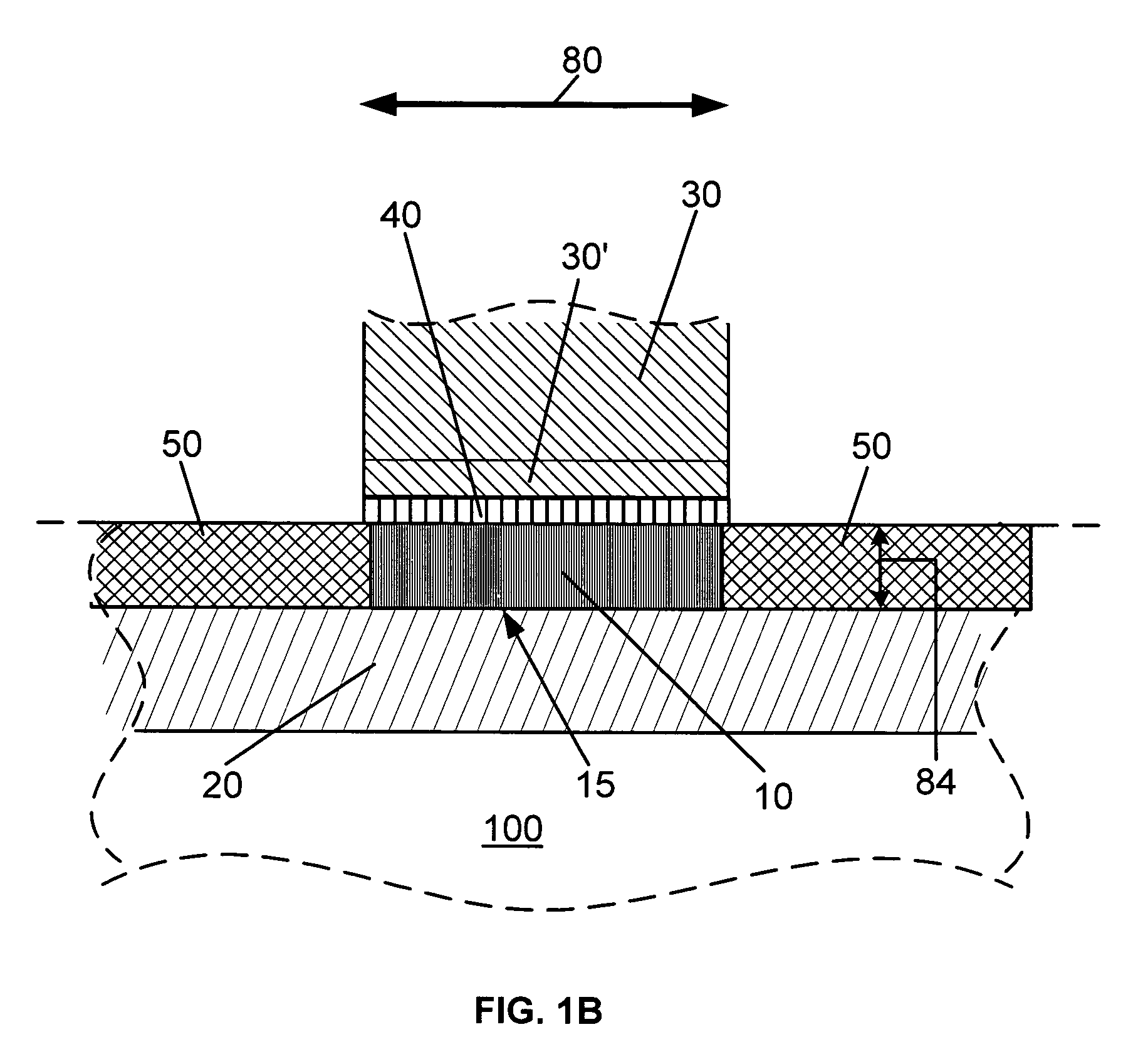
[0019]FIG. 1A and FIG. 1B show, in a schematic cross sectional view, exemplary embodiments of ultra short, less than about 40 nm gate length MOSFET devices. The depicted embodiments incorporate elements that are instrumental in achieving useful characteristics for such ultra short gate length MOSFET devices. Embodiments of the present invention are aimed at gate lengths less than about 40 nm, with the 15 nm to 35 nm regime being preferred. It is also preferred that a mid-gap workfunction metal be the material which is in direct contact with the gate insulator. The metal gate electrode is preferred due to its high carrier concentration, which leads to low gate resistance and high gate capacitance. The term “mid-gap” means that the workfunction of the gate material, in the presented embodiments the metal, has a workfunction which is roughly halfway between the workfunctions of the p-type and n-type versions of the semiconductor material which forms the MOSFET. The workfunction of the ...


PUM


Abstract

MOSFET devices suitable for operation at gate lengths less than about 40 nm, and methods of their fabrication is being presented. The MOSFET devices include a ground plane formed of a monocrystalline Si based material. A Si based body layer is epitaxially disposed over the ground plane. The body layer is doped with impurities of opposite type than the ground plane. The gate has a metal with a mid-gap workfunction directly contacting a gate insulator layer. The gate is patterned to a length of less than about 40 nm, and possibly less than 20 nm. The source and the drain of the MOSFET are doped with the same type of dopant as the body layer. In CMOS embodiments of the invention the metal in the gate of the NMOS and the PMOS devices may be the same metal.

Description

FIELD OF THE INVENTION[0001]The present invention relates to electronic devices. In particular it relates to less than 40 nm gate length field effect devices and methods of producing such structures.BACKGROUND OF THE INVENTION[0002]Today's integrated circuits include a vast number of devices. Smaller devices and shrinking ground rules are the key to enhance performance and to improve reliability. As FET (Field Effect Transistor) devices are being scaled down, the technology becomes more complex, and changes in device structures and new fabrication methods are needed to maintain the expected performance enhancement from one generation of devices to the next. The mainstay material of microelectronics is silicon (Si), or more broadly, Si based materials. One such Si based material of importance for microelectronics is the silicon-germanium (SiGe) alloy.[0003]There is great difficulty in maintaining performance improvements in devices of deeply submicron generations. Various detrimental...

Claims


Application Information

Patent Timeline
Patent Type & Authority Patents(United States)
IPC IPC(8): H01L29/76
CPCH01L21/28017H01L29/105H01L29/7838
Inventor CHU, JACK OONDORIS, BRUCE B.IEONG, MEIKEIWANG, JING
Owner GLOBALFOUNDRIES INC
Why Eureka
Try Eureka