Enhanced compliant probe card systems having improved planarity

a probe card and compliant technology, applied in the direction of semiconductor/solid-state device testing/measurement, coupling device connection, instruments, etc., can solve the problems of inability to meet the requirements of the test, etc., to achieve high parallel testing levels, reduce assembly manufacturing cost and manufacturing time, and extend mechanical compliance

Inactive Publication Date: 2008-03-25
ADVANTEST SINGAPORE PTE LTD
View PDF385 Cites 110 Cited by
  • Summary
  • Abstract
  • Description
  • Claims
  • Application Information

AI Technical Summary

Benefits of technology

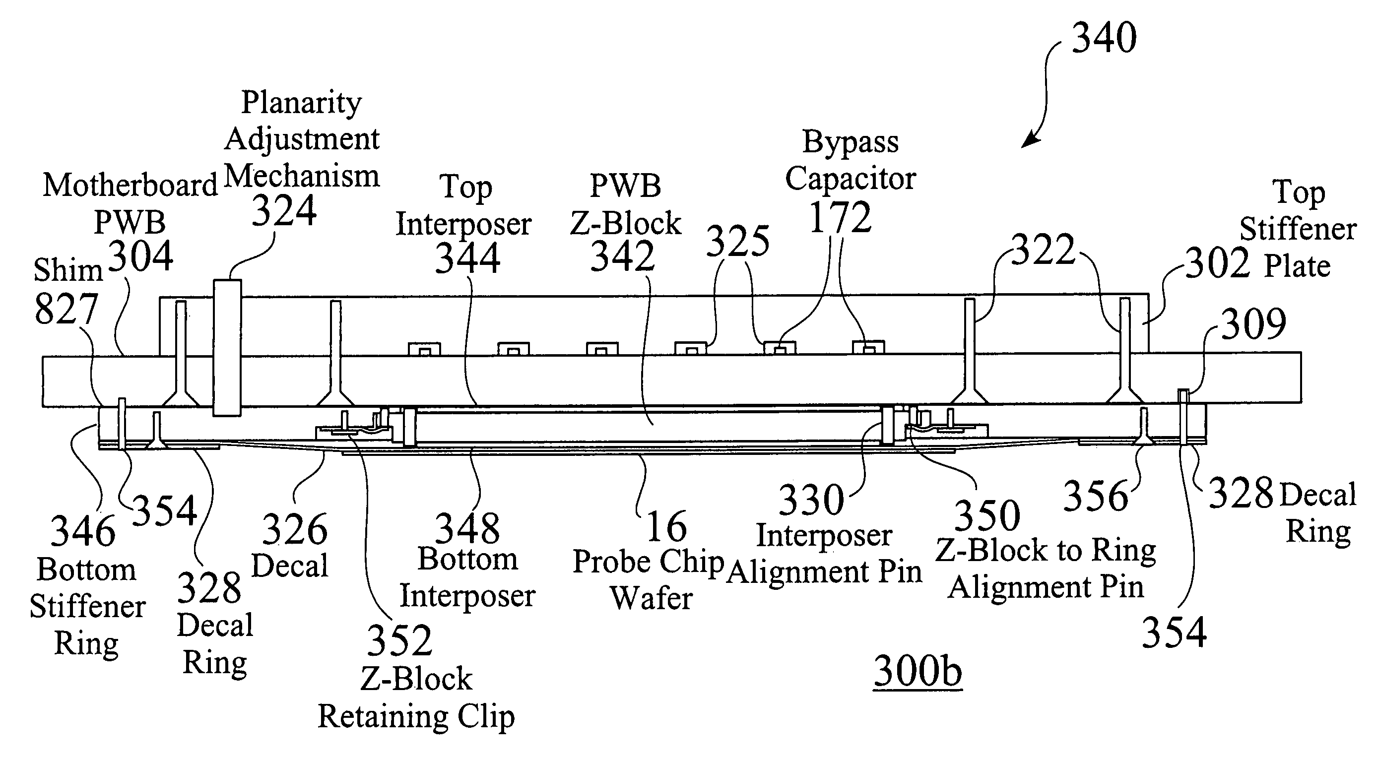
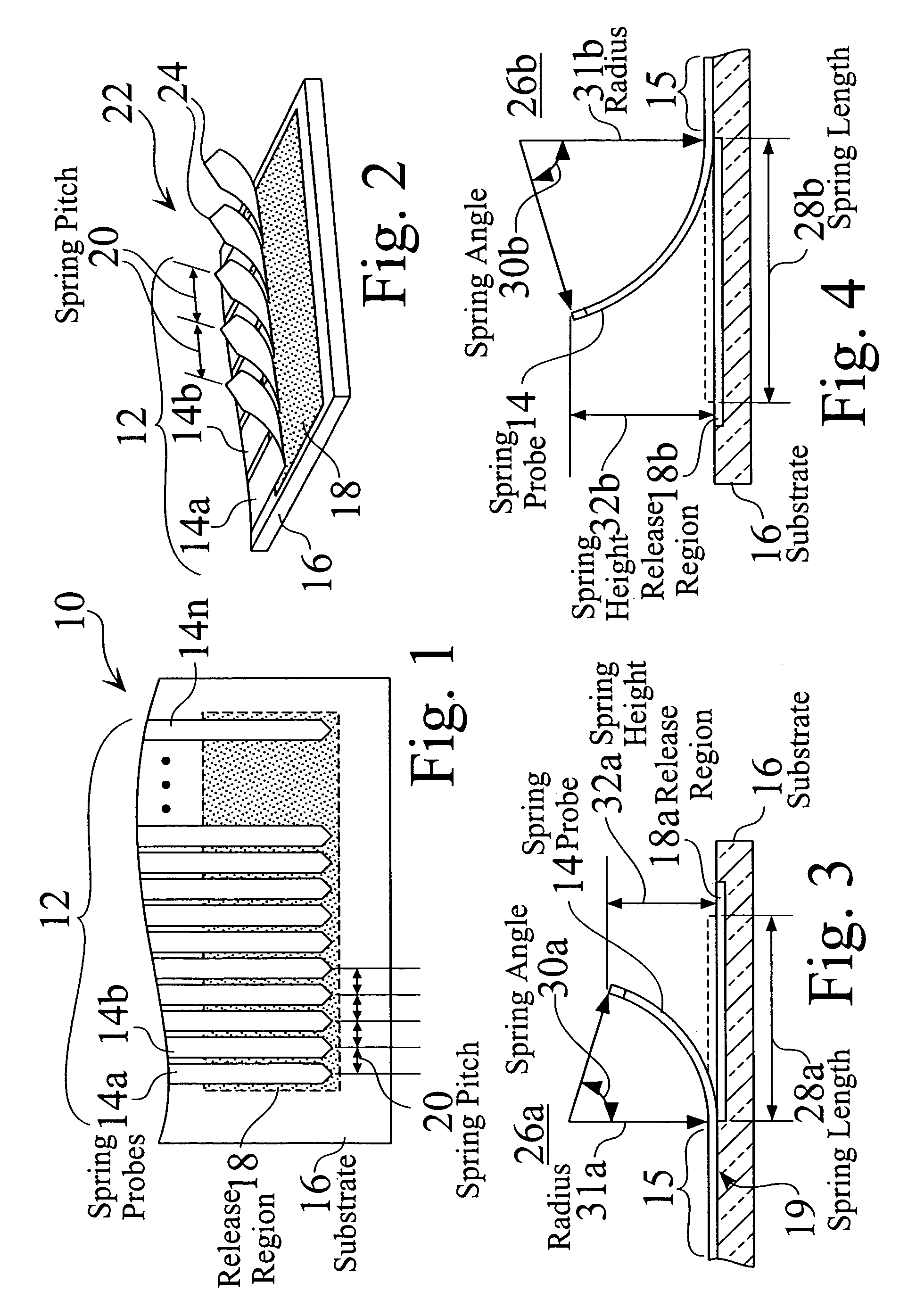
[0034]Several embodiments of enhanced integrated circuit probe card assemblies are disclosed, which extend the mechanical compliance of both MEMS and thin-film fabricated probes, such that these types of spring probe structures can be used to test one or more integrated circuits on a semiconductor wafer. Several embodiments of probe card assemblies, which provide tight signal pad pitch compliance and / or enable high levels of parallel testing in commercial wafer probing equipment, are disclosed. In some preferred embodiments, the probe card assembly structures include separable standard components, which reduce assembly manufacturing cost and manufacturing time. These structures and assemblies enable high speed testing in wafer form. The probes also have built in mechanical protection for both the integrated circuits and the MEMS or thin film fabricated spring tips and probe layout structures on substrates. Alternate card assembly structures comprise a stiffening structure and a compliant carrier structure, such as a decal or screen, which is attached to the probe chip substrate.

Problems solved by technology

However, advanced semiconductor technologies often require higher pin counts, smaller pad pitches, and higher dock frequencies, which are not possible with tungsten needle probes.
While emerging technologies have provided spring probes for different probing applications, most probes have inherent limitations, such as limited pitch, limited pin count, varying levels of flexibility, limited probe tip geometries, limitations of materials, and high costs of fabrication.
As a result, there is even greater component density but without interference of wire bonds one with the other, this factor of interference being the previous limiting factor in achieving high component density networks in a multi layer ceramic package”.
While the contact tip structures disclosed by B. Eldridge et al. provide resilient contact structures, the structures are each individually mounted onto bond pads on semiconductor dies, requiring complex and costly fabrication.
As well, the contact tip structures are fabricated from wire, which often limits the resulting geometry for the tips of the contacts.
Furthermore, such contact tip structures have not been able to meet the needs of small pitch applications (e.g. typically on the order of 50 μm spacing for a peripheral probe card, or on the order of 75 μm spacing for an area array).
While the photolithography patterned springs, as disclosed by Smith et al., are capable of satisfying many IC probing needs, the springs are small, and provide little vertical compliance to handle the planarity compliance needed in the reliable operation of many current IC prober systems.
Furthermore, no one has taught a way to interconnect such a probe containing up to several thousand pins to a tester, while effectively dealing with planarity requirements.
Microprocessor devices are some of the IC devices which are most severely limited by today's IC packages.
Conventional packages using wire bonds or solder ball attachments have both signal and power parasitics, which impact performance.
Current wire bond and solder ball technologies cannot maintain signals in the 20 GHz range.
Packages using wire bonds and solder balls attachments have signal, power and ground parasitics that impact performance.
This BBUL and MCM approaches tend to be very expensive due to fabrication complexity, and the need to guarantee that every chip in the module is good.
Any bad chip or defect in manufacturing of the HDI between chips will cause all of the chips and the package to be rejected.
A bad chip is any chip that does not meet performance requirements.
Resultant BBUL / MCM packages are therefore typically significantly more expensive to manufacture than individually packaged ICs.
In the past, the “chips-first” approach was only used to build MCMs used in satellites for space applications, where the smaller size and weight justified the higher cost.

Method used


Image

  • Enhanced compliant probe card systems having improved planarity
  • Enhanced compliant probe card systems having improved planarity
  • Enhanced compliant probe card systems having improved planarity

Examples


first embodiment

[0443]Two preferred embodiments are currently contemplated. the invention uses a low-count mosaic comprised of a few probe chips, for example four probe chips. The probe chips have the same TCE as the wafer under test, e.g. silicon. In this embodiment, the probe chip is peripherally attached to the membrane.

second embodiment

[0444]the invention provides a high-count mosaic, using a high number of probe chips, for example nine or more probe chips. In this embodiment, the probe chips are smaller and can have a slight TCE difference from that of the test wafer, e.g. silicon. For example, the probe chips may be made out of a ceramic material. This embodiment of the invention uses a center attachment to secure the probe chips to the membrane.

[0445]Other embodiments with different TCE matching characteristics and probe chip sizes could benefit from attaching at both the central and peripheral areas to the membrane.

[0446]FIG. 98 and FIG. 99 show a low-count mosaic starting substrate 1200, 1210, which is fabricated using known techniques to provide an array of die site regions, each having contacts formed on a first surface 62a thereof that are complementary to the die pads of devices to be tested and / or burned in on a test wafer. Contacts are also formed on a second, opposite surface 62b of the die site region...


PUM

PropertyMeasurementUnit
sizeaaaaaaaaaa
temperaturesaaaaaaaaaa
frequenciesaaaaaaaaaa

Abstract

Several embodiments of enhanced integrated circuit probe card and package assemblies are disclosed, which extend the mechanical compliance of both MEMS and thin-film fabricated probes, such that these types of spring probe structures can be used to test one or more integrated circuits on a semiconductor wafer. Several embodiments of probe card assemblies, which provide tight signal pad pitch compliance and / or enable high levels of parallel testing in commercial wafer probing equipment, are disclosed. In some preferred embodiments, the probe card assembly structures include separable standard components, which reduce assembly manufacturing cost and manufacturing time. These structures and assemblies enable high speed testing in wafer form. The probes also have built in mechanical protection for both the integrated circuits and the MEMS or thin film fabricated spring tips and probe layout structures on substrates. Alternate card assembly structures comprise a stiffening structure and a compliant carrier structure, such as a decal or screen, which is fixedly attached to the probe chip substrate.

Description

CROSS REFERENCE TO RELATED APPLICATIONS[0001]This Application is a Continuation In Part of U.S. patent application Ser. No. 10 / 178,103 (NNEX0001CIP), entitled Construction Structures and Manufacturing Processes for Probe Card Assemblies and Packages Having Wafer Level Springs, U.S. Filing Date 24 Jun. 2002, now U.S. Pat. No. 6,917,525, which is a Continuation in Part of U.S. patent application Ser. No. 09 / 980,040 (nnex0003), entitled Construction Structures and Manufacturing Processes for Integrated Circuit Wafer Probe Card Assemblies, U.S. Filing Date 27 Nov. 2001, now U.S. Pat. No. 6,799,976, which claims priority from PCT Patent Application Ser. No. PCT / US00 / 21012 (NNEX0003P), filed Jul. 27, 2000; and from PCT Patent Application Ser. No. PCT / US00 / 14164 (NNEX0001P), entitled Construction Structures and Manufacturing Processes for Integrated Circuit Wafer Probe Card Assemblies, U.S. Filing Date 23 May 2000.[0002]This Application is also a Continuation In Part of U.S. patent applica...

Claims


Application Information

Patent Timeline
Patent Type & Authority Patents(United States)
IPC IPC(8): H05K7/06G01R1/067G01R1/073G01R3/00G01R31/28H05K3/40H05K7/10
CPCG01R1/07314H05K7/1061G01R1/06711G01R3/00Y10T29/49004G01R1/06727Y10S439/912H05K3/4092
Inventor HAEMER, JOSEPH MICHAELCHONG, FU CHIUNGMODLIN, DOUGLAS N.
Owner ADVANTEST SINGAPORE PTE LTD
Why Eureka
Try Eureka