Integrated memory circuit arrangement

a memory circuit and integrated technology, applied in the field of memory circuit arrangement, can solve the problems of comparatively small voltage drop and power loss, voltage drop, and not substantially impair the operation of the circuit arrangement, and achieve the effect of simple construction and good electrical properties

Inactive Publication Date: 2008-03-25
INFINEON TECH AG
View PDF18 Cites 9 Cited by
  • Summary
  • Abstract
  • Description
  • Claims
  • Application Information

AI Technical Summary

Benefits of technology

[0011]The switching element provides degrees of freedom that permit new operating modes of the memory circuit arrangement. By way of example, it is possible to carry the same potential on the disconnected voltage feed in a plurality or even in all of the operating modes. The switching power required for changing the potential becomes lower.
[0013]In a next embodiment, the bit lines are local bit lines that can be electrically conductively connected to global bit lines via further switching elements. The local bit lines define a memory segment by virtue of the fact that they are connected only to a portion of the cells of a column of the memory circuit arrangement. The circuit arrangement contains at least two memory segments. The use of memory segments affords the possibility of driving the memory circuit arrangement in a similar manner to a magnetic storage disk that likewise contains segments. Moreover, what is achieved by the use of local and global bit lines is that the global bit lines can be arranged in upper metallization layers and, by way of example, have a larger cross-section than the local bit lines or the distance with respect to one another is increased. The former reduces the bit line resistance (R) and the latter reduces the capacitive load (C) of the bit lines. As a result, the RC delay due to the global bit lines is shorter and the access times of the circuit arrangement are improved. The use of memory segments additionally affords the simple possibility of limiting the length of the local bit lines, in particular of the local bit lines routed in doped regions.
[0015]In another embodiment, the switching element is arranged at an end of a row of memory cells of a column of a memory segment. Alternatively or in addition, the switching element is arranged between the memory cells of a column of a memory segment, preferably in the center of the column, in order to feed a current into two equal length sections of the bit lines arranged in a doped region. The voltage drop across the bit line in the doped region can thus be reduced further in a simple way.
[0017]In particular, a combination of the two circuit arrangements according to the invention leads to a circuit arrangement of simple construction which has particularly good electrical properties, for example, with regard to the power consumption. Moreover, operating modes are again made possible with potential conditions which would require additional lines in the column direction without the combination. Furthermore, the required chip area is small on account of the combination.
[0018]In one embodiment, the circuit arrangement contains a control unit, which drives the switching elements for connecting two bit lines alternately to the switching elements for connecting the collective line to the bit line. The alternate driving ensures that no potential conflicts occur on a bit line.

Problems solved by technology

The metal line has a smaller resistance in comparison with a doped region, so that leading the operating voltage as far as the switching element is associated with a comparatively small voltage drop and power loss.
If a bit line comprises metal, then the disadvantages associated with the use of doped regions with regard to the specific conductivity and a voltage drop associated therewith do not occur at least with regard to these bit lines.
Moreover, what can be achieved by using a plurality of switching elements per column or by skillful arrangement of the switching element or of the switching elements, for example on half the length of the two bit lines, is that the disadvantages associated with the doped region do not substantially impair the operation of the circuit arrangement.

Method used


Image

  • Integrated memory circuit arrangement
  • Integrated memory circuit arrangement
  • Integrated memory circuit arrangement

Examples


Embodiment Construction

[0027]Identical, functionally identical, or similar elements and signals are referred to with the same reference symbols in the figures unless stated otherwise.

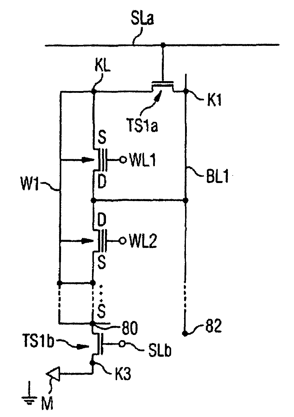
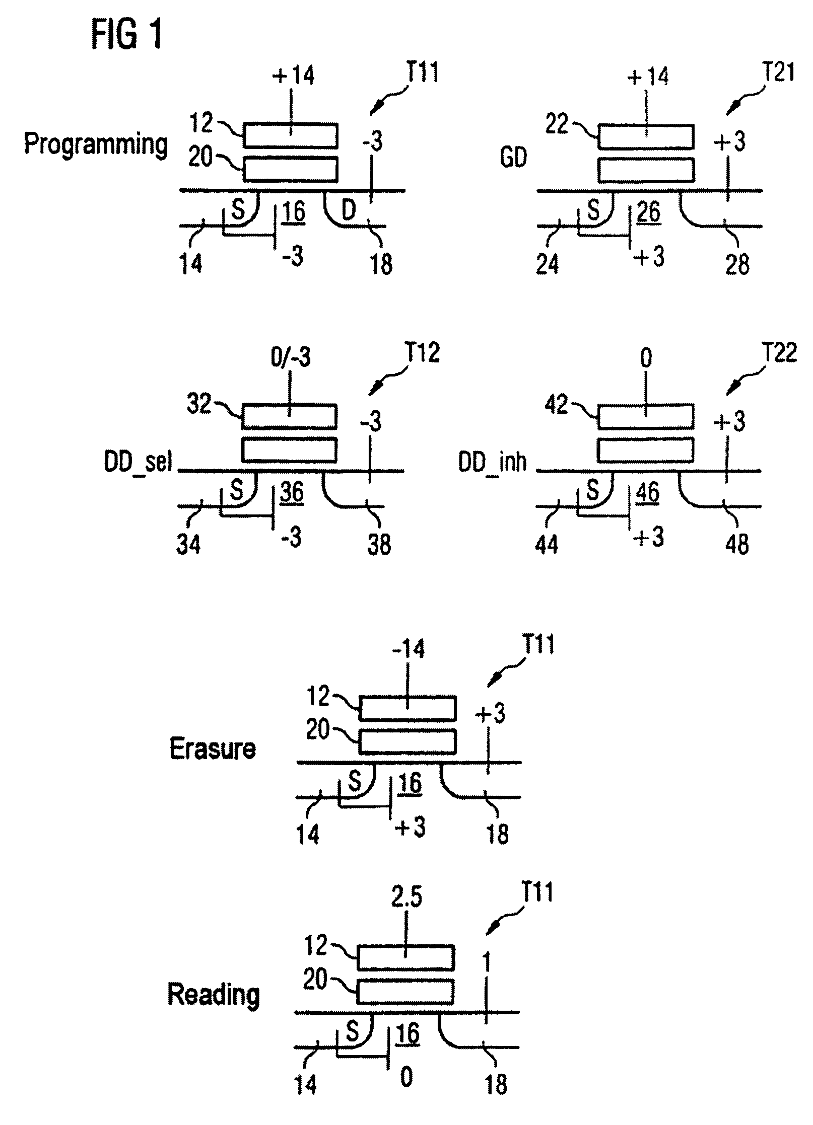
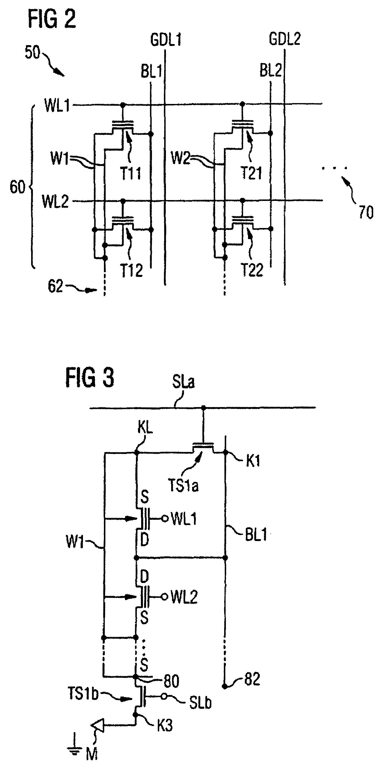
[0028]FIG. 1 shows an exemplary embodiment of voltage conditions at memory cells during programming, during erasing and during reading of memory cells of a circuit arrangement explained in greater detail below with reference to FIGS. 2 to 4. The voltage values cited in connection with FIG. 1 are only examples and may be chosen deviating within wide limits from the voltage values cited, e.g. deviating by plus or minus 50% or 30% of the respective voltage value. Operating modes with fundamentally different voltage values can also be realized. In the explanation of FIG. 1, reference is made to memory transistors T11 to T22, the arrangement of which in a memory cell array is explained in more detail below with reference to FIG. 2. The memory transistor T11 is chosen by way of example for explaining the operating modes. It goes wi...


PUM


Abstract

A memory circuit arrangement includes a switching element per column that can be used to connect or disconnect two bit lines for memory cells of a column. The switching element leads to a reduction of the chip area and / or to an improvement in the electronic properties of the memory circuit arrangement.

Description

PRIORITY AND CROSS REFERENCE TO RELATED APPLICATION[0001]This application is a continuation of International Application No. PCT / EP2004 / 050356 filed Mar. 24, 2004, which claims priority to German application 103 23 244.3, filed May 22, 2003, both of which are incorporated in their entirety by reference herein.BACKGROUND OF THE INVENTION[0002]1. Field of the Invention[0003]The invention relates to a memory circuit arrangement, and in particularly to a memory arrangement having a switching element for connection of bit lines for memory cells.[0004]2. Description of the Related Art[0005]Memory cells of a memory circuit are arranged in rows and columns or in matrix-type fashion. Each memory cell has a transistor that may have a floating gate. Word lines and bit lines are transversely arranged where the word lines are electrically connected to control electrodes (also referred to as the gate) of the transistors of a row. The bit lines are connected to terminal electrodes of the transisto...

Claims


Application Information

Patent Timeline
Patent Type & Authority Patents(United States)
IPC IPC(8): G11C5/06G11C11/34G11C7/12G11C16/04G11C16/24H01L27/115
CPCG11C7/12G11C16/0416G11C16/24H01L27/115H10B69/00
Inventor TEMPEL, GEORG
Owner INFINEON TECH AG
Why Eureka
Try Eureka