High-efficiency light-emitting element

a light-emitting element, high-efficiency technology, applied in the direction of semiconductor laser structure details, electrical equipment, semiconductor devices, etc., can solve the problems of increasing both the difficulty of the led process and the cost, and reducing the light transmission distance. , the effect of increasing the total light-emitting area

Active Publication Date: 2008-04-08
EPISTAR CORP
View PDF22 Cites 52 Cited by
  • Summary
  • Abstract
  • Description
  • Claims
  • Application Information

AI Technical Summary

Benefits of technology

[0009]Because the lattice orientation of the nitride material has a hexagonal character, the hexagonal-pyramid cavity can be generated in the nitride material with the lattice character. The hexagonal-pyramid cavity formed on the surface not only increases the total light-emitting area, but also decreases the light loss due to the total reflection when the light generated from the light-emitting layer passes through the surface. In addition, because the hexagonal-pyramid cavity extends from the surface downward, the light that emits into the hexagonal-pyramid cavity would not decay due to the absorption of the semiconductor material. That is, the present invention can reduce the light transmission distance in the upper semiconductor layer of the light-emitting layer and reduce the possibility of being absorbed by the semiconductor material so as to improve the light-emitting efficiency of the light-emitting element.

Problems solved by technology

However, the light generated from an LED is not easily emitted from the LED.
However these prior arts techniques require complicated manufacturing processes, which increases both the difficulty of the LED process and the cost.
So these prior arts can solve the problem of the total reflection but they cannot overcome the light absorption of the semiconductor layer.

Method used


Image

  • High-efficiency light-emitting element
  • High-efficiency light-emitting element
  • High-efficiency light-emitting element

Examples


embodiment 1

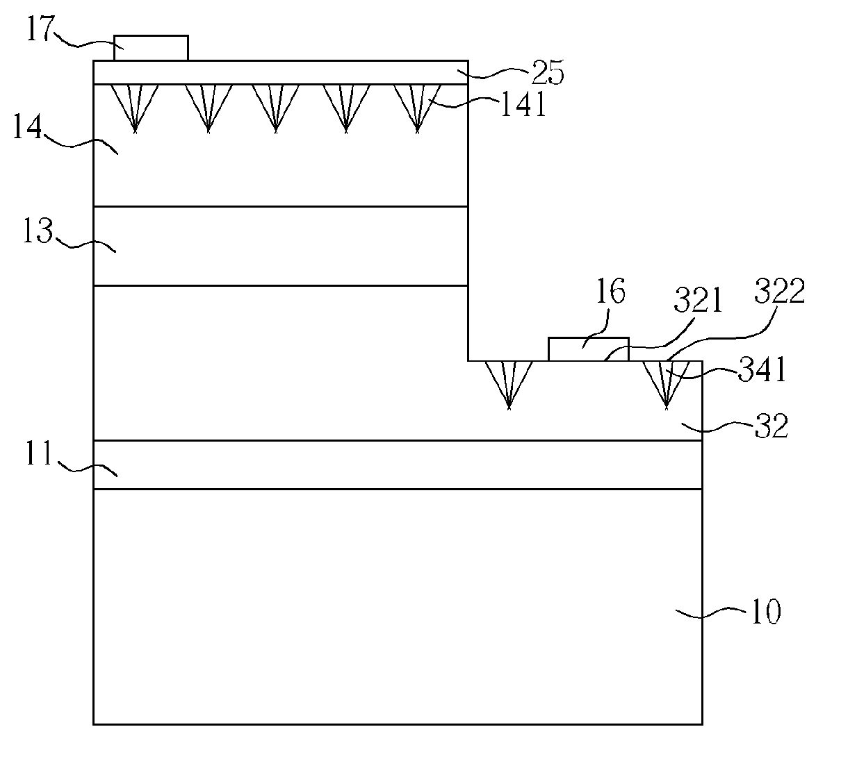
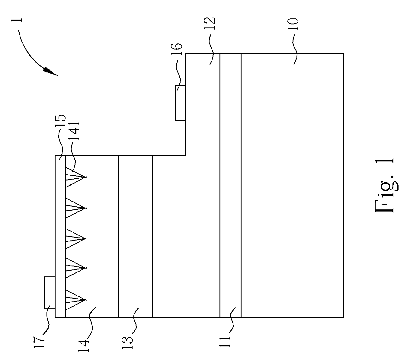
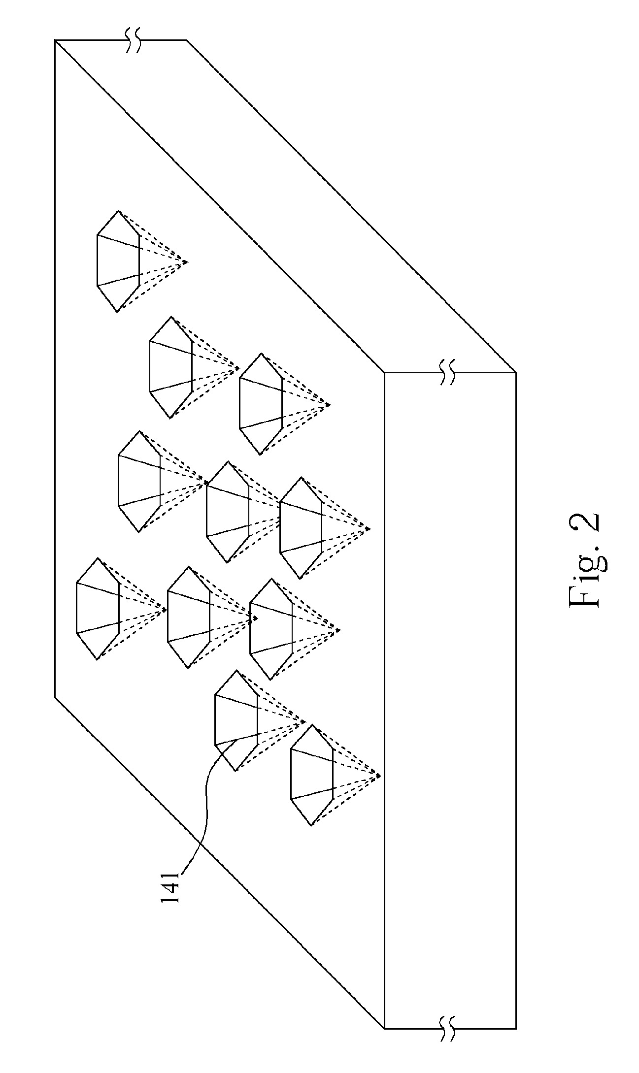
[0020]Please refer to FIG. 1. FIG. 1 is a diagram of a high-efficiency light-emitting element 1 according to a first embodiment of the present invention. The high-efficiency light-emitting element 1 includes a sapphire substrate 10, a nitride buffer layer 11 formed on the sapphire substrate 10, and a n-type nitride semiconductor layer 12 formed on the nitride buffer layer 11. The n-type nitride semiconductor layer 12 includes a first surface and a second surface distant from the nitride buffer layer 11. The high-efficiency light-emitting element 1 further includes a nitride multiple-quantum well light-emitting layer 13 formed on the first surface, and a p-type nitride semiconductor layer 14 formed on the nitride multiple-quantum well light-emitting layer 13. The p-type nitride semiconductor layer 14 includes a plurality of hexagonal-pyramid cavities 141 on the surface and a distance from the nitride multiple-quantum well light-emitting layer 13, wherein the hexagonal-pyramid cavity ...

embodiment 2

[0022]The configuration of embodiment 2 is similar to embodiment 1, and the difference between embodiment 1 and embodiment 2 is as follows, the initial layers of the hexagonal-pyramid cavities 141 grow between the epitaxial temperature 700° C. and 950° C. for changing the crystal nucleation so as to form the hexagonal-pyramid cavities 141 on the surface of the p-type nitride semiconductor layer 14 or inside the p-type nitride semiconductor layer 14. The variation of the epitaxial growth temperature and the heating or cooling can determine the size and the density of the plurality of hexagonal-pyramid cavities 141 so as to change the light-emitting efficiency.

embodiment 3

[0023]The configuration of embodiment 3 is similar to embodiment 1, and the difference between embodiment 1 and embodiment 3 is as follows, the p-type nitride semiconductor layer is grown in a nitrogen rich environment for changing the crystal nucleation so as to form the hexagonal-pyramid cavities 141 on the surface of the p-type nitride semiconductor layer 14 or inside the p-type nitride semiconductor layer 14. The modulation of the epitaxial growth environment and the proportion of the nitrogen, hydrogen, and nitrogen source can determine the size and the density of the plurality of hexagonal-pyramid cavities 141 so as to change the light-emitting efficiency.


PUM


Abstract

A high-efficiency light-emitting element includes a substrate, a first nitride semiconductor layer formed on the substrate, a nitride light-emitting layer formed on the first nitride semiconductor layer, and a second nitride semiconductor layer formed on the nitride light-emitting layer including a plurality of hexagonal-pyramid cavities on the surface of the second nitride semiconductor layer opposite to the nitride light-emitting layer.

Description

BACKGROUND OF INVENTION[0001]1. Field of the Invention[0002]The present invention relates to a light-emitting element, and more particularly, to a high-efficiency light-emitting element.[0003]2. Description of the Prior Art[0004]The applications of light-emitting diodes are extensive and include optical display devices, traffic signals, data storing devices, communication devices, illumination devices, and medical apparatuses.[0005]The conventional light-emitting diode includes a substrate, a first electrode semiconductor layer formed on the substrate, a light-emitting layer formed on the first electrode semiconductor layer, a second electrode semiconductor layer formed on the light-emitting layer, and a transparent conductive layer formed on the second electrode semiconductor layer. LED light travels in each direction instead of focusing on one place. However, the light generated from an LED is not easily emitted from the LED. According to Snell's law, only light emitted at an angl...

Claims


Application Information

Patent Timeline
Patent Type & Authority Patents(United States)
IPC IPC(8): H01L31/12H01L27/15H01L33/06H01L33/12H01L33/24H01L33/32H01L33/42H01S5/02
CPCH01L33/32H01L33/22H01L33/20
Inventor OU, CHENLIN, TING-YANGCHANG, JIA-RONGLAI, SHIH-KUO
Owner EPISTAR CORP
Why Eureka
Try Eureka