Interposer and method for fabricating the same

a technology of interposers and components, which is applied in the field of interposers, can solve the problems of large inductance due to the wiring of lines, difficult to reduce the cost by the techniques described in patent references 1 to 5, and achieves good electric characteristics, high electrostatic capacitance, and good relative dielectric constant.

Inactive Publication Date: 2008-04-08
FUJITSU LTD
View PDF12 Cites 20 Cited by
  • Summary
  • Abstract
  • Description
  • Claims
  • Application Information

AI Technical Summary

Benefits of technology

[0029]According to the present invention, the thin-film capacitors are formed, using a highly heat-resistant semiconductor substrate, which permits the capacitor dielectric film to be well crystallized and have a high relative dielectric constant of 200 or above. Thus, according to the present invention, the thin-film capacitors having very good electric characteristics can be formed. Furthermore, according to the present invention, the semiconductor substrate, which is difficult to have through-holes formed in, is removed, which makes it unnecessary to form in the semiconductor substrate the through-holes for the through-electrodes to be buried in. Thus, the present invention can provide an interposer including thin-film capacitors of very high electrostatic capacitance at low costs.

Problems solved by technology

However, in mounting the decoupling capacitors near the LSI mounted on a circuit wiring board, the LSI and the decoupling capacitors are electrically connected to each other via lines formed on the circuit wiring board, and accordingly large inductance due to the wiring of the lines is present.
It is not easy to form the through-holes in the substrate.
Accordingly, it is very difficult to decrease the cost by the techniques described in Patent References 1 to 5.
In the technique described in Patent Reference 6, the capacitors are formed by forming films on an organic film (resin layer), which makes it impossible to form the dielectric film of good crystalline material.
Thus, the capacitors cannot have high relative dielectric constant.

Method used


Image

  • Interposer and method for fabricating the same
  • Interposer and method for fabricating the same
  • Interposer and method for fabricating the same

Examples


first embodiment

A First Embodiment

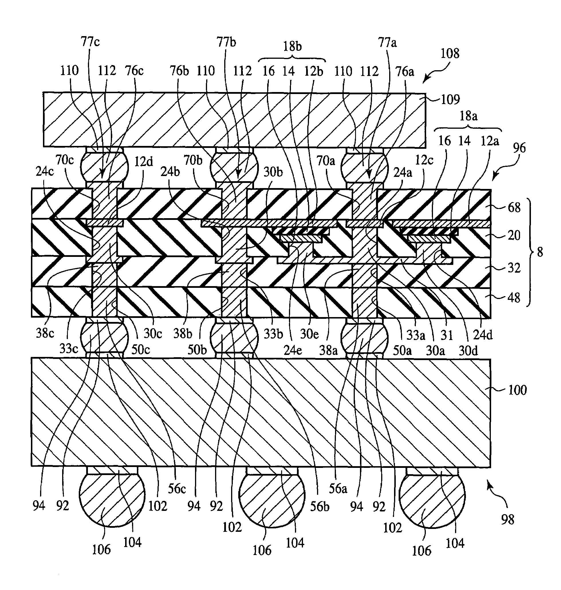
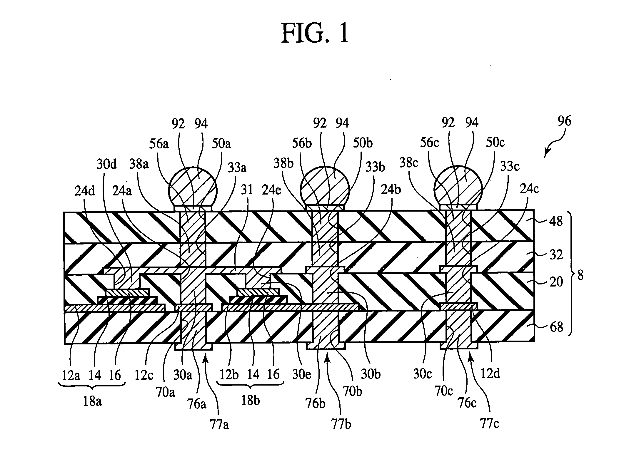
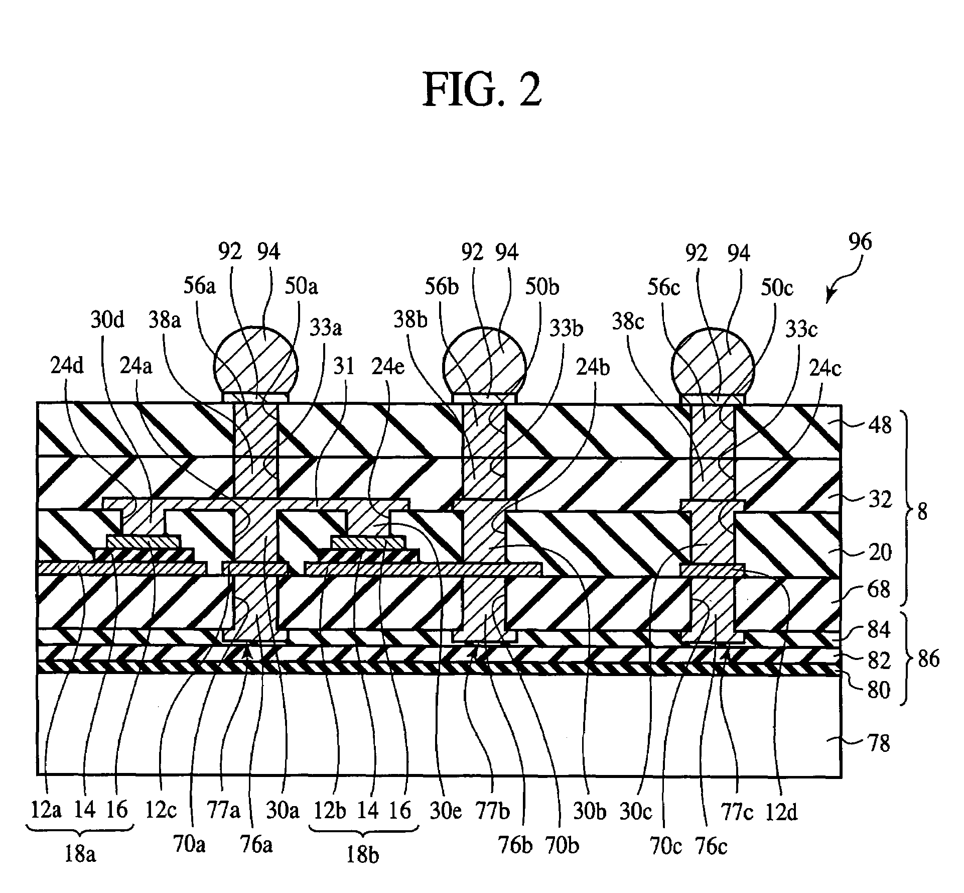
[0117]The interposer according to a first embodiment of the present invention and the method for fabricating the interposer, and an electronic device using the interposer and a method for fabricating the electronic device will be explained with references from FIGS. 1 to 30.

[0118](Interposer and Electronic Device)

[0119]First, the interposer and the electronic device according to the present embodiment and the electronic device will be explained with reference to FIGS. 1 to 3. FIG. 1 is a sectional view of the interposer according to the present embodiment (Part 1). FIG. 2 is a sectional view of the interposer according to the present embodiment (Part 2). FIG. 3 is a sectional view of the electronic device according to the present embodiment.

[0120]As illustrated in FIG. 1, the interposer 96 according to the present embodiment comprises a base 8 of a plurality of resin layers 68, 20, 32, 48 laid the latter on the former, thin film capacitors 18a, 18b buried in the ba...

second embodiment

A Second Embodiment

[0378]The interposer according to a second embodiment of the present invention and the method for fabricating the interposer, the electronic device using the interposer and the method for fabricating the electronic device will be explained with references from to FIGS. 36 to 62. The same members of the present embodiment as those of the interposer according to the first embodiment and the method for fabricating the interposer, etc. are represented by the same reference numbers not to repeat or to simplify their explanation.

[0379](Interposer and Electronic Device)

[0380]First, the interposer according to the present embodiment, and the electronic device using the interposer will be explained with reference to FIGS. 36 to 38. FIG. 36 is a sectional view (Part 1) of the interposer according to the present embodiment. FIG. 37 is a sectional view (Part 2) of the interposer according to the present embodiment. FIG. 38 is a sectional view of the electronic device accordin...

third embodiment

A Third Embodiment

[0535]The interposer according to a third embodiment of the present invention and the method for fabricating the interposer, and the electronic device using the interposer and the method for fabricating the electronic device will be explained with references from FIGS. 63 to 87. The same members of the present embodiment as those of the interposer according to the first and the second embodiments and the method for fabricating the interposers, etc. illustrated in FIGS. 1 to 62 are represented by the same reference numbers not to repeat or to simplify their explanation.

[0536](Interposer and Electronic Device)

[0537]First, the interposer and the electronic device according to the present embodiment will be explained with reference to FIGS. 63 to 65. FIG. 63 is a sectional view of the interposer according to the present embodiment (Part 1). FIG. 64 is a sectional view of the interposer according to the present embodiment (Part 2). FIG. 65 is a sectional view of the ele...


PUM


Abstract

The interposer comprises a base 8 formed of a plurality of resin layers 68, 20, 32, 48; thin-film capacitors 18a, 18b buried between a first resin layer 68 of said plurality of resin layers and a second resin layer 20 of said plurality of resin layers, which include first capacitor electrodes 12a, 12b, second capacitor electrodes 16 opposed to the first capacitor electrode 12a, 12b and the second capacitor electrode 16, and a capacitor dielectric film 14 of a relative dielectric constant of 200 or above formed between the first capacitor electrode 12a, 12b and the second capacitor electrode 16; a first through-electrode 77a formed through the base 8 and electrically connected to the first capacitor electrode 12a, 12b; and a second through-electrode 77b formed through the base 8 and electrically connected to the second capacitor electrode 16.

Description

CROSS-REFERENCE TO RELATED APPLICATION[0001]This application is based upon and claims priority of Japanese Patent Application No. 2005-286978, filed on Sep. 30, 2005, the contents being incorporated herein by reference.BACKGROUND OF THE INVENTION[0002]The present invention relates to an interposer and a method for fabricating the interposer, more specifically an interposer including a capacitor dielectric film of very high relative dielectric constant formed in, and a method for fabricating the interposer.[0003]Recently, for digital LSI's (Large Scale Integrated circuits), etc., typically microprocessors, etc., the operation speed is increased, and the electric power consumption is decreased.[0004]To stably operate the LSI's in the GHz-band high-frequency range and furthermore at low voltage, it is very important to suppress the source voltage fluctuations due to abrupt changes of load impedance, etc. of the LSI's and to remove high-frequency noises of the power source.[0005]Convent...

Claims


Application Information

Patent Timeline
Patent Type & Authority Patents(United States)
IPC IPC(8): H01L23/29
CPCH01L21/4846H01L23/49822H01L23/50H01L23/642H01L23/645H05K1/162H01L21/4857Y10T29/42H01L21/6835H01L2224/16H01L2924/01046H01L2924/01077H01L2924/01078H01L2924/01079H01L2924/15311H01L2924/3011H05K1/165H05K3/0023H05K3/0044H05K3/20H05K3/4614H05K2201/0175H05K2201/0179H05K2201/0317H05K2201/09481H05K2201/09509H05K2201/096H05K2201/09763H05K2201/10674H05K2203/016H05K2203/0733H01L2224/16235Y10T29/4913Y10T29/49155Y10T29/49156Y10T29/435Y10T29/49126Y10T29/49002H01L2224/05573H01L2224/05568H01L2924/00014H01L2224/05599
Inventor SHIOGA, TAKESHIISHIZUKI, YOSHIKATSUNAKAGAWA, KANAESAKAI, TAIJIMIZUKOSHI, MASATAKABANIECKI, JOHN DAVIDKURIHARA, KAZUAKI
Owner FUJITSU LTD
Why Eureka
Try Eureka