
Soft error resistant memory cell and method of manufacture

Active Publication Date: 2008-04-08
LONGITUDE FLASH MEMORY SOLUTIONS LTD
View PDF7 Cites 6 Cited by
  • Summary
  • Abstract
  • Description
  • Claims
  • Application Information

AI Technical Summary

Benefits of technology

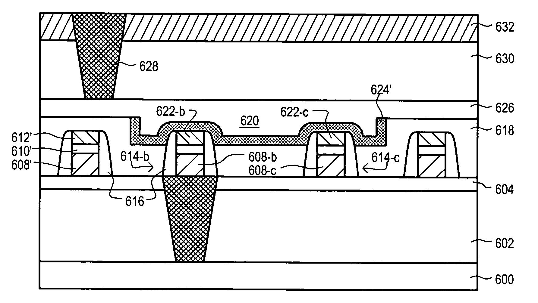
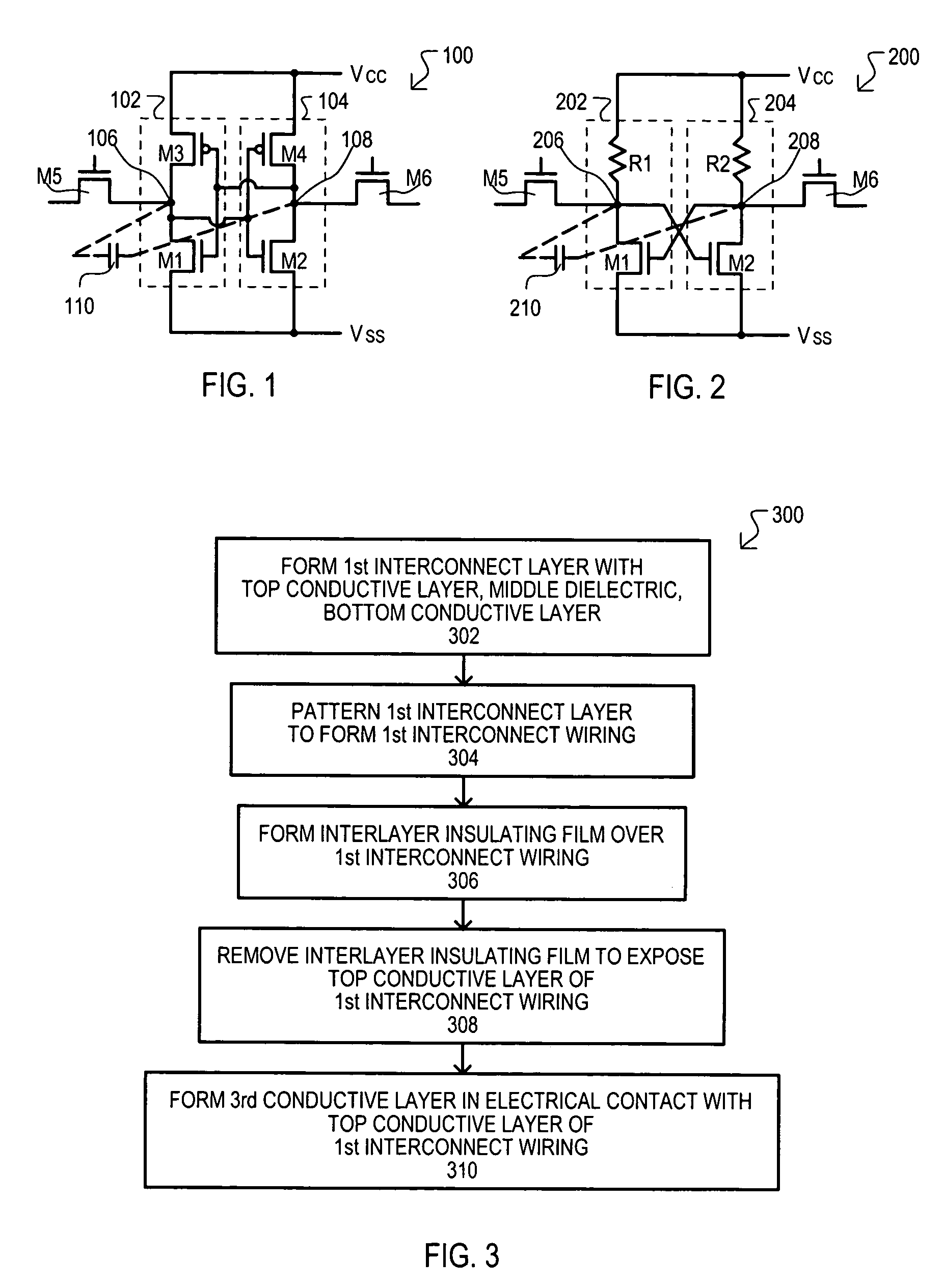
[0010]The inclusion of a capacitor between data storage nodes can increase a memory cell resistance to soft error events (i.e., reduce a soft error rate).
[0016]In this way, a capacitor can be formed from memory cell wiring utilized to connect memory cell circuit components. Such an arrangement may advantageously utilize existing structures within a memory cell.
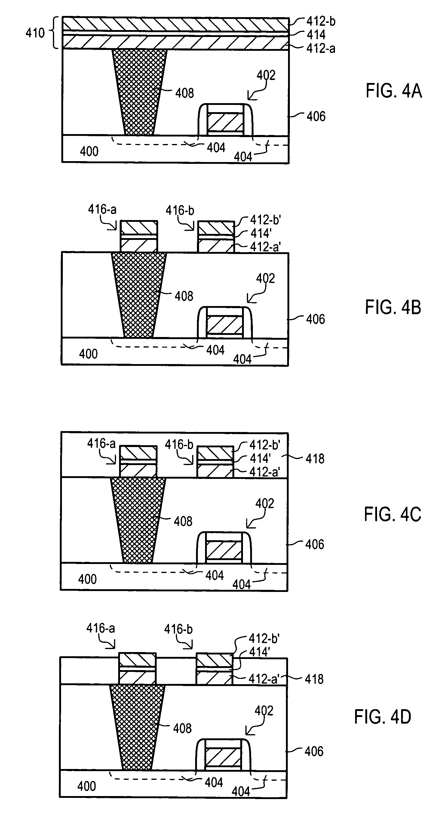
[0028]In this way, a spacer can be formed that can isolate a bottom layer of a first interconnect wiring from a top layer. Such an arrangement can make it easier to make a conductive connection with a top conductive layer while maintaining electrical isolation from a bottom conductive layer of the interconnect wiring.

Problems solved by technology

Unfortunately, semiconductor memory devices are still vulnerable to errors that may arise out of the operating environment and conditions, such as “soft” errors.
More particularly, many soft errors are believed to result from alpha particles traveling through a semiconductor substrate and generating electron hole pairs.
In a soft-error event, generated electron hole pairs can cause a change in state of the data stored within a memory device.
For example, in the case of a dynamic random access memory (DRAM) type cell, generated electron hole pairs may result in loss of charge from a storage capacitor.
However, this approach has disadvantages that may include increased current consumption and / or larger memory cell sizes.
Unfortunately, as semiconductor memory devices continue to shrink in size, the number of electron hole pairs necessary to induce a soft error can be correspondingly smaller.

Method used


Image

  • Soft error resistant memory cell and method of manufacture
  • Soft error resistant memory cell and method of manufacture
  • Soft error resistant memory cell and method of manufacture

Examples


Embodiment Construction

[0046]Various embodiments of the present invention will now be described in detail with reference to a number of drawings. The embodiments include a memory cell circuit having a capacitor for reducing a soft error rate, as well as a method of manufacturing such a capacitor.

[0047]A first embodiment of the present invention includes a memory cell and is set forth in FIG. 1 and designated by the general reference character 100. A first embodiment 100 can include a memory cell having a built-in capacitor for increasing a capacitance between data storage nodes. Such an increased capacitance can reduce a soft-error rate (SER) by improving a node's resistance to being charged / discharged in response to a soft error event (e.g., spontaneous generation of electron-hole pairs). In the very particular example of FIG. 1, a memory cell can include a static random access memory (SRAM) type memory cell. However, the present invention should not necessarily be construed as being limited to any parti...


PUM


Abstract

A semiconductor device memory cell (100) can include a built-in capacitor for reducing a soft-error rate (SER). A memory cell (100) can include a first inverter (102) and second inverter (104) arranged in a cross-coupled configuration. A capacitor (110) can be coupled between a first storage node (106) and second storage node (108). A capacitor (110) can be a “built-in” capacitor formed with interconnect wirings utilized to connect memory cell circuit components.

Description

[0001]This application claims the benefit of U.S. provisional patent application Ser. No. 60 / 463,430, filed Apr. 16, 2003.TECHNICAL FIELD[0002]The present invention relates generally to integrated circuits and, more particularly to a circuit for reducing a soft-error rate in a semiconductor memory device, and a method of manufacturing such a circuit.BACKGROUND OF THE INVENTION[0003]Semiconductor memory devices are typically manufactured with circuits, such as redundancy circuits, to address defects that can arise from uncontrollable manufacturing process variations, and the like. Unfortunately, semiconductor memory devices are still vulnerable to errors that may arise out of the operating environment and conditions, such as “soft” errors.[0004]“Soft” errors are random errors that can appear in a memory device that are not related to any defect. Soft errors are most often attributed, either directly or indirectly, to sub-atomic particles. More particularly, many soft errors are belie...

Claims


Application Information

Patent Timeline
IPC IPC(8): G11C11/24
CPCG11C11/4125H01L27/11H01L27/1104Y10S257/903H10B10/00H10B10/12
Inventor JIN, BOCHATILA, AHMADWONG, KAICHIU
Owner LONGITUDE FLASH MEMORY SOLUTIONS LTD
Learn More