Material composition analysis system and method

a composition analysis and composition technology, applied in the field of semiconductor metrology, can solve the problems of insufficient selectiveness, insufficient selection, and inability to effectively determine the material properties of a multi-layer film stack, and achieve the effect of accurately and accurately determining the phase of specific device layers

Inactive Publication Date: 2008-04-15
KLA TENCOR TECH CORP
View PDF1 Cites 30 Cited by
  • Summary
  • Abstract
  • Description
  • Claims
  • Application Information

AI Technical Summary

Benefits of technology

[0011]Conventional systems and methods cannot effectively determine the material properties of a thin film within a multi-layer film stack. Typical nondestructive phase determination systems (e.g., XRF and XRD) are too slow, too imprecise (i.e., large spot size), and are not selective enough to provide phase detection utility in a production environment. Destructive techniques (e.g., TEM and SIMS), while able to accurately determine the phase of specific device layers, are by definition not suitable for use on in-line production monitoring. To overcome these limitations of conventional systems and techniques, an electron probe microanalysis system can be used in conjunction with layer thickness measurement data to efficiently and accurately determine material phase without any wafer-damaging effects.

Problems solved by technology

Conventional systems and methods cannot effectively determine the material properties of a thin film within a multi-layer film stack.
Typical nondestructive phase determination systems (e.g., XRF and XRD) are too slow, too imprecise (i.e., large spot size), and are not selective enough to provide phase detection utility in a production environment.
Destructive techniques (e.g., TEM and SIMS), while able to accurately determine the phase of specific device layers, are by definition not suitable for use on in-line production monitoring.

Method used


Image

  • Material composition analysis system and method
  • Material composition analysis system and method
  • Material composition analysis system and method

Examples


Embodiment Construction

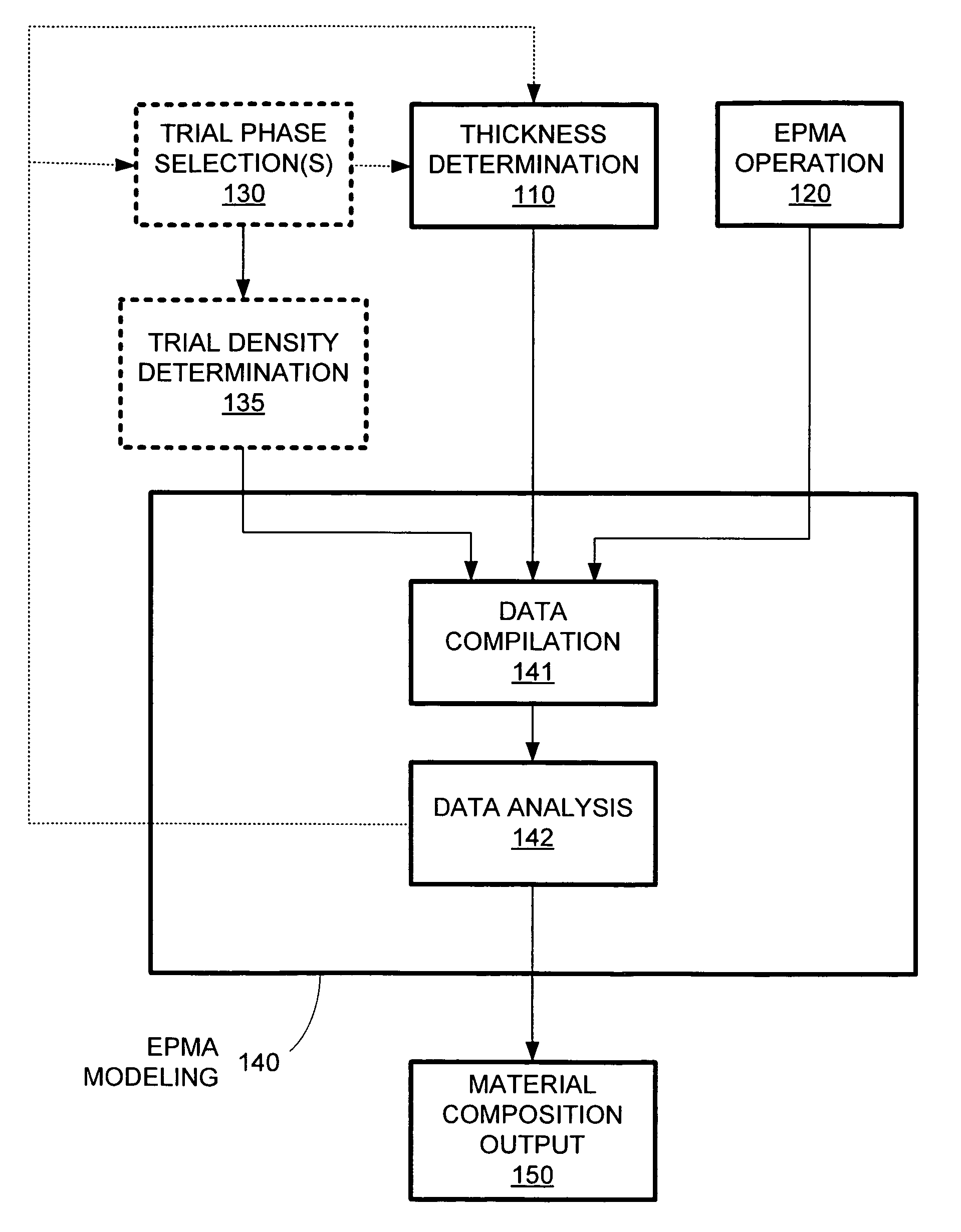
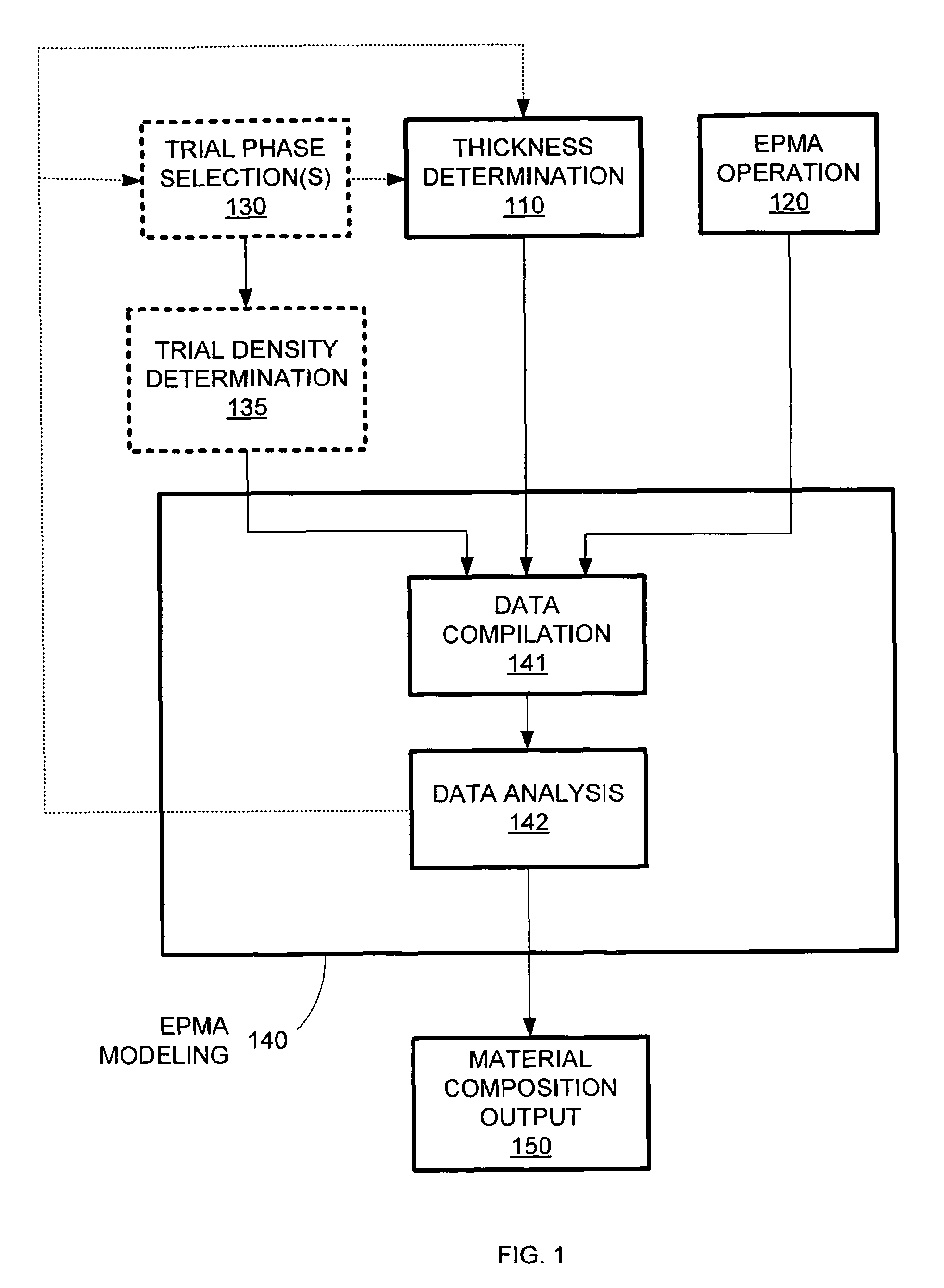
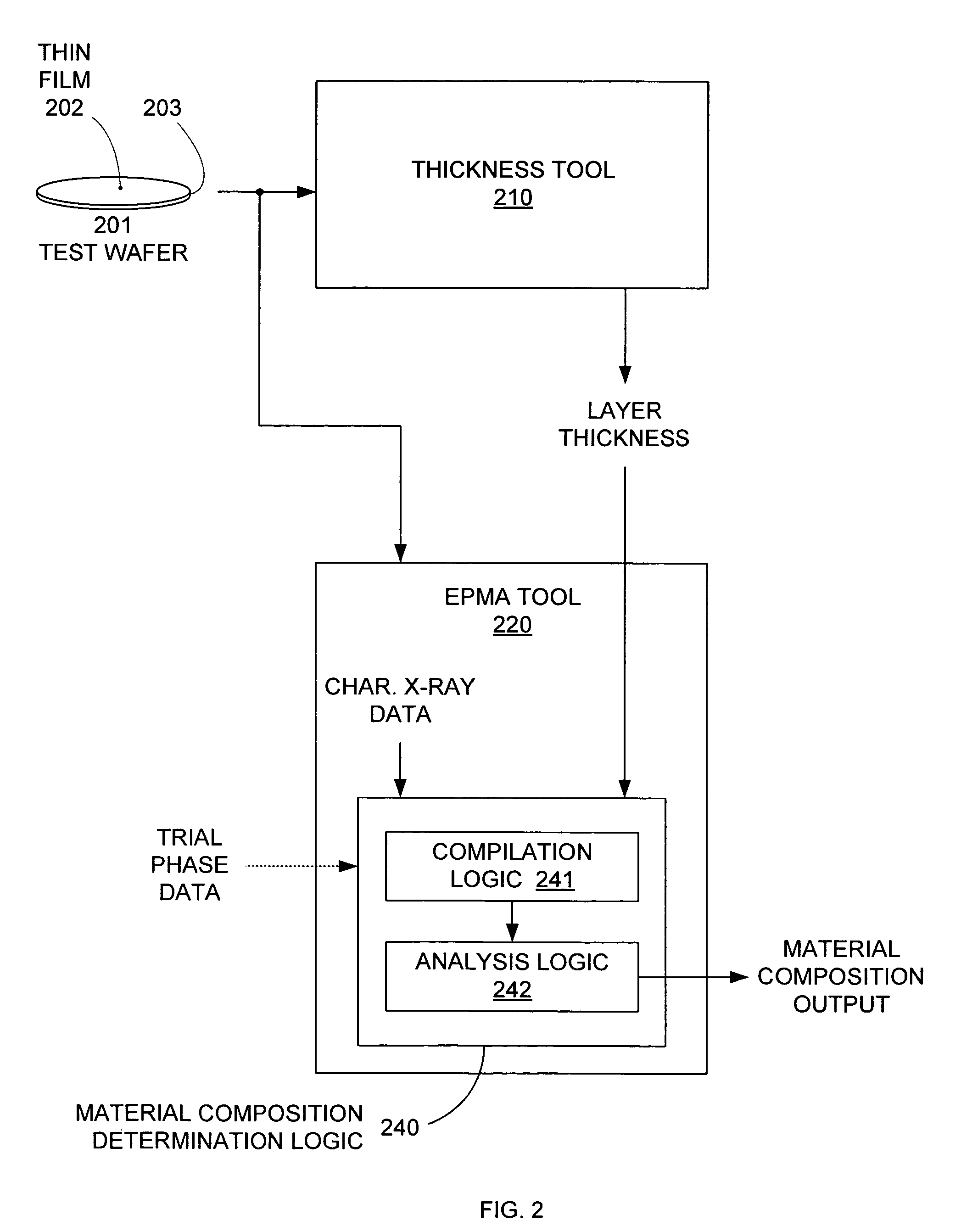
[0018]Conventional systems and methods cannot effectively determine the material properties of a thin film formed on a multi-layer film stack that shares an element with top thin film. Typical nondestructive phase determination systems (e.g., XRF and XRD) are too slow, too imprecise (i.e., large spot size), and are not selective enough to provide accurate material composition determinations in a production environment. Destructive techniques (e.g., TEMS and SIMS) that can provide such material composition information are by definition not suitable for use in production line environments. To overcome these limitations of conventional systems and techniques, an electron probe microanalysis system can be used in conjunction with layer thickness data to efficiently and accurately determine material phase without any wafer-damaging effects.

[0019]Electron probe microanalysis (EPMA), which is sometimes referred to as electron microprobe analysis (EMPA), involves the measurement of characte...


PUM

PropertyMeasurementUnit
sizeaaaaaaaaaa
densitiesaaaaaaaaaa
densitiesaaaaaaaaaa

Abstract

The material composition of a thin film formed on a substrate or covered by a cap layer that shares one or more elements with the thin film can be determined by combining characteristic material data, such as characteristic x-ray data, from a material composition analysis tool, such as an electron probe-based x-ray metrology (EPMA) operation, with thickness data and (optionally) possible material phases for the thin film. The thickness data and / or the material phase options can be used to determine, for example, the penetration depth of a probe e-beam of the EPMA tool. Based on the penetration depth and the thin film thickness, the characteristic x-ray data from the EPMA operation can be analyzed to determine the composition (e.g., phase or elemental composition) of the thin film. An EPMA tool can include ellipsometry capabilities for all-in-one thickness and composition determination.

Description

BACKGROUND OF THE INVENTION[0001]1. Field of the Invention[0002]The invention relates to the field of semiconductor metrology, and in particular, to thin film composition determination including phase identification in multilayer structures.[0003]2. Related Art[0004]As modern semiconductor device geometries continue to shrink, performing metrology (i.e., determining material composition properties such as elemental distribution or molecular structure (phase)) on those devices becomes increasingly important and difficult. Currently, some of the most problematic metrology operations involve the analysis of multilayer stacks (e.g., a thin film on a substrate or multiple thin films formed on top of each other) that share one or more common elements. Conventional metrology techniques can have difficulty determining the material composition properties of such “shared element” structures since conventional techniques cannot readily distinguish between signals from the common element that o...

Claims


Application Information

Patent Timeline
Patent Type & Authority Patents(United States)
IPC IPC(8): G01N23/00
CPCG01N23/227
Inventor GAO, YINGSARFATY, MOSHE
Owner KLA TENCOR TECH CORP
Why Eureka
Try Eureka