Reducing cracking of high-lead or lead-free bumps by matching sizes of contact pads and bump pads

a technology of contact pads and bump pads, which is applied in the direction of basic electric elements, electrical apparatus construction details, solid-state devices, etc., can solve the problems of high-speed off-chip interconnection, toxic materials, and excessive brittleness of inter-metallic components, so as to reduce stress, improve the reliability of the resulting assembly, and the effect of extra effor

Active Publication Date: 2008-04-22
MICROSOFT TECH LICENSING LLC
View PDF7 Cites 133 Cited by
  • Summary
  • Abstract
  • Description
  • Claims
  • Application Information

AI Technical Summary

Benefits of technology

[0011]In accordance with one aspect of the present invention, a semiconductor package assembly comprises a contact pad (first conductive pad) or an under bump metallurgy (UBM) on a semiconductor substrate, a bump underlying the contact pad and overlying a package substrate, which has a bump pad (second conductive pad) in contact with the bump. A top interface exists between the contact pad / UBM and the bump, and a bottom interface exists between the bump and a bump pad of the package substrate. The sizes of the top and bottom interfaces are substantially comparable. The balanced structure reduces stress applied to the bump, the inter-metallic component and neighboring materials. The reliability of the resulting assembly is significantly improved.
[0012]The preferred embodiment of the present invention has presented a packaging solution that solves the cracking problem for lead-free and high-lead-containing bumps. The solution is compatible with the present packaging process. There is no extra effort or cost introduced. Also there is no requirement of using high strength underfills to protect bumps, therefore, damage to low-k materials in the chip is avoided.

Problems solved by technology

Eliminating bond wires reduces the delay in inductance and capacitance of the connection, and substantially shortens the current path, resulting in a high-speed off-chip interconnection.
Lead is a toxic material.
However, the commonly known lead-free solder, such as Sn—Ag, Sn—Ag—Cu and their inter-metallic components are too brittle, therefore, suffering cracking.
High-lead bumps are also brittle and each prone to cracking.
The coefficient of thermal expansion (CTE) mismatch between materials in the package assembly is one of the main reasons causing stress.
With low-k dielectrics widely used in the integrated circuit, a dilemma exists between the protection of bumps and low-k dielectrics.
However, the low-k dielectrics may be harmed by high strength underfill material and problems such as delaminating occur.

Method used


Image

  • Reducing cracking of high-lead or lead-free bumps by matching sizes of contact pads and bump pads
  • Reducing cracking of high-lead or lead-free bumps by matching sizes of contact pads and bump pads
  • Reducing cracking of high-lead or lead-free bumps by matching sizes of contact pads and bump pads

Examples


Embodiment Construction

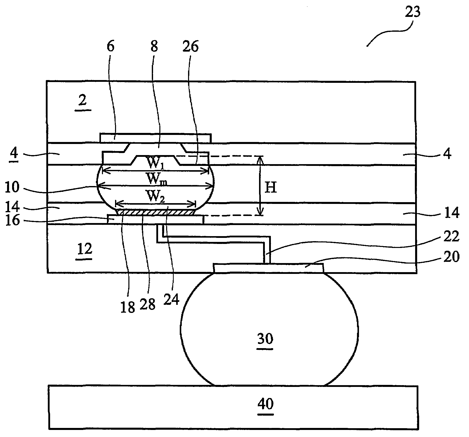
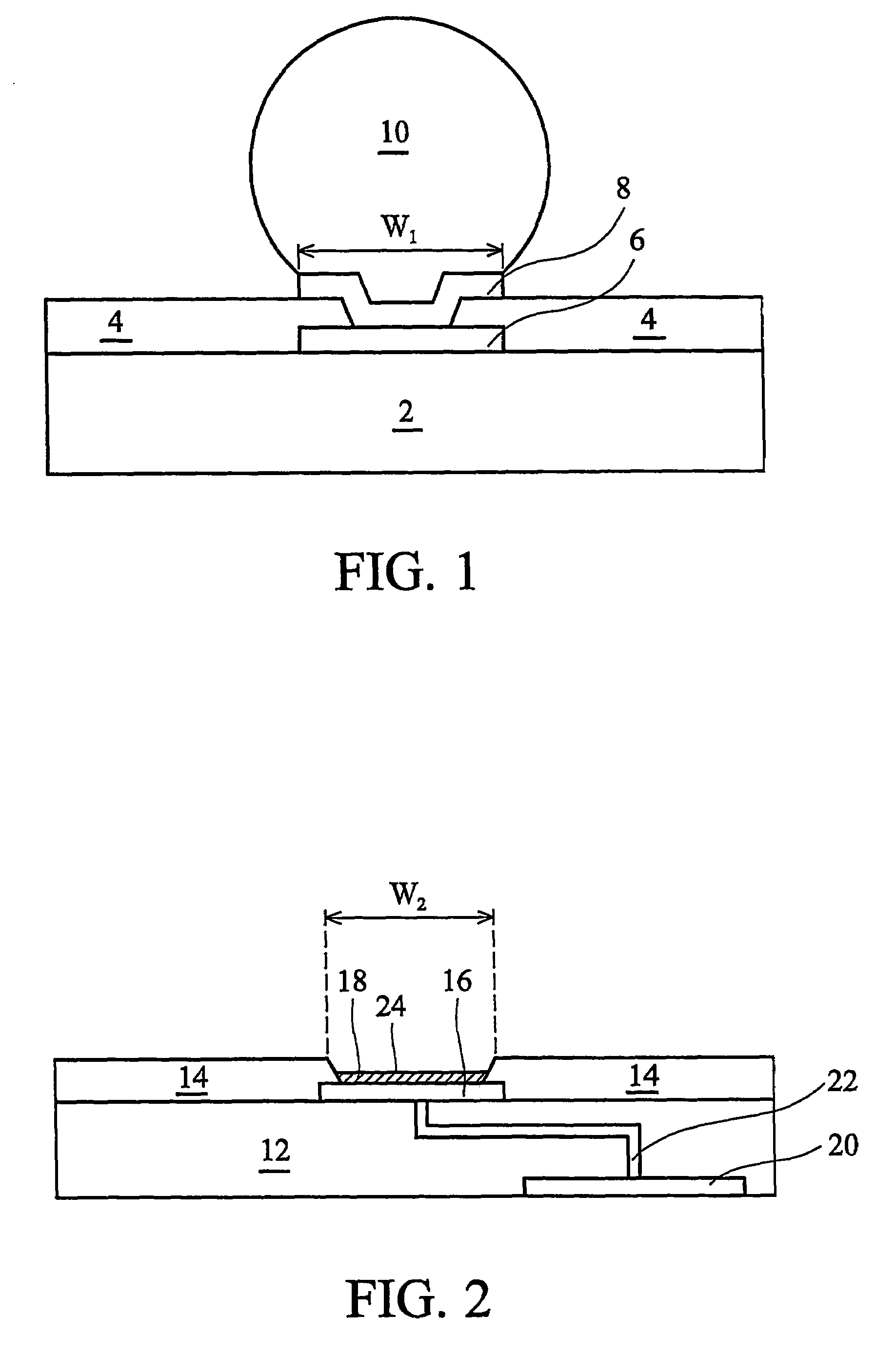
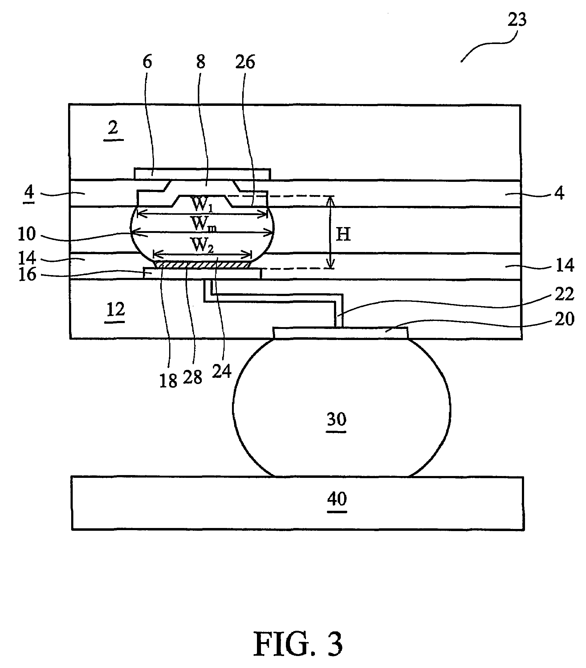
[0017]The making and using of the presently preferred embodiments are discussed in detail below. It should be appreciated, however, that the present invention provides many applicable inventive concepts that can be embodied in a wide variety of specific contexts. The specific embodiments discussed are merely illustrative of specific ways to make and use the invention, and do not limit the scope of the invention.

[0018]The preferred embodiment of the present invention presents a package assembly structure that uses lead-free or high-lead-containing bumps. The preferred embodiments are illustrated in FIGS. 1 through 4 wherein like reference numbers are used to designate like elements throughout the various views and illustrative embodiments of the present invention.

[0019]In the preferred embodiment, solder bumps are formed on chips, which contain integrated circuits. In other embodiments, the solder bumps are formed on package substrates. FIG. 1 illustrates a semiconductor substrate 2 ...


PUM


Abstract

A semiconductor package assembly comprises a first conductive pad on a semiconductor substrate; a second conductive pad on a package substrate; a bump physically coupled between the first conductive pad and the second conductive pad, wherein the bump is substantially lead-free or high-lead-containing; the bump has a first interface with the first conductive pad, the first interface having a first linear dimension; the bump has a second interface with the second conductive pad, the second interface having a second linear dimension; and wherein the ratio of the first linear dimension and the second linear dimension is between about 0.7 and about 1.7.

Description

TECHNICAL FIELD[0001]This invention relates generally to integrated circuit packaging, more particularly to a method of forming electrically conductive bumps for flip chip packages.BACKGROUND[0002]A flip chip microelectronic assembly includes a direct electrical connection of facing-down (that is, “flipped”) electronic components onto substrates, such as ceramic substrates, circuit boards, or carriers using conductive bump bond pads of the chip. Flip chip technology is quickly replacing older wire bonding technology that uses facing-up chips with a wire connected to each pad on the chip.[0003]The flip chip components used in flip chip microelectronic assemblies are predominantly semiconductor devices, however, components such as passive filters, detector arrays, and memory devices are also being used in flip chip form. Flip chips are advantageous because of their high-speed electrical performance when compared to other assembly methods. Eliminating bond wires reduces the delay in in...

Claims


Application Information

Patent Timeline
Patent Type & Authority Patents(United States)
IPC IPC(8): H01L23/48H01L21/00H05K7/10
CPCH01L23/3114H01L23/49816H01L24/13H01L24/10H01L2924/10253H01L2924/014H01L2224/13099H01L2924/01013H01L2924/01015H01L2924/01027H01L2924/01029H01L2924/01033H01L2924/01046H01L2924/01051H01L2924/01074H01L2924/01075H01L2924/01078H01L2924/01079H01L2924/01082H01L2924/01322H01L2924/14H01L2924/30105H01L2924/30107H01L2924/01006H01L2924/01019H01L2924/01047H01L2924/01087H01L2924/00H01L24/16H01L2224/05124H01L2224/05147H01L2224/05559H01L2224/05571H01L2224/05572H01L2224/05647H01L2224/05655H01L2224/05664H01L2224/13H01L2924/00011H01L2924/15787H01L2924/00014H01L2924/00012H01L2224/81805H01L2924/013
Inventor LU, SZU WEILEE, HSIN-HUIWANG, CHUNG YULII, MIRNG-JI
Owner MICROSOFT TECH LICENSING LLC
Why Eureka
Try Eureka