Laser beam processing method and laser beam machine

a laser beam machine and laser beam technology, applied in the field of laser beam processing method and laser, can solve the problems of reducing productivity, difficult cutting with the above cutting blade, and large area ratio of streets to wafers

Active Publication Date: 2008-04-29
DISCO CORP
View PDF6 Cites 120 Cited by
  • Summary
  • Abstract
  • Description
  • Claims
  • Application Information

AI Technical Summary

Benefits of technology

[0010]It is an object of the present invention to provide a laser beam processing method and a laser beam machine, which are capable of dividing a wafer into parallelogram or trapezoid chips by using a laser beam processing technique, even when streets formed on the wafer are narrow in width.
[0016]In the present invention, since the laser beam is applied to the wafer at a predetermined angle toward a direction intersecting at right angles to the processing-feed direction relative to a direction perpendicular to the surface, to which the laser beam is applied, of the wafer to form deteriorated layers in the inside of the wafer, even when the streets formed on the wafer are narrow in width, the wafer can be divided into parallelogram or trapezoid chips. Further, in the laser beam machine of the present invention, as only the condenser of the laser beam application means may be tilted, a mechanism for tilting is simple.

Problems solved by technology

Further, since a sapphire substrate, silicon carbide substrate, lithium tantalite substrate and the like have a high Mohs hardness, cutting with the above cutting blade is not always easy.
Therefore, in the case of a device measuring about 300 μm×300 μm, the area ratio of the streets to the wafer is large, thereby reducing productivity.

Method used


Image

  • Laser beam processing method and laser beam machine
  • Laser beam processing method and laser beam machine
  • Laser beam processing method and laser beam machine

Examples


Embodiment Construction

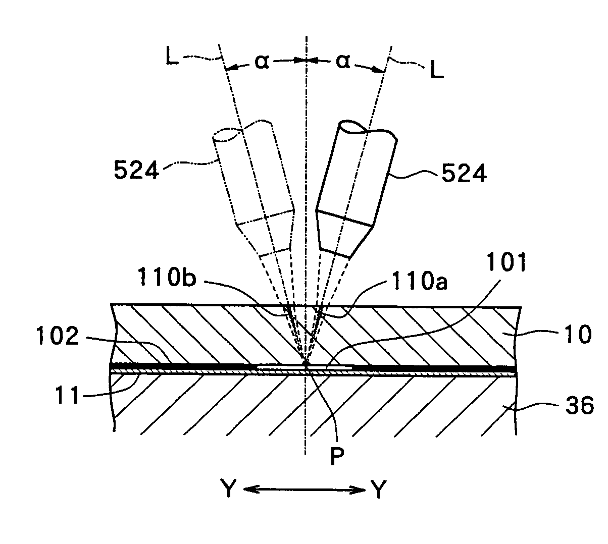
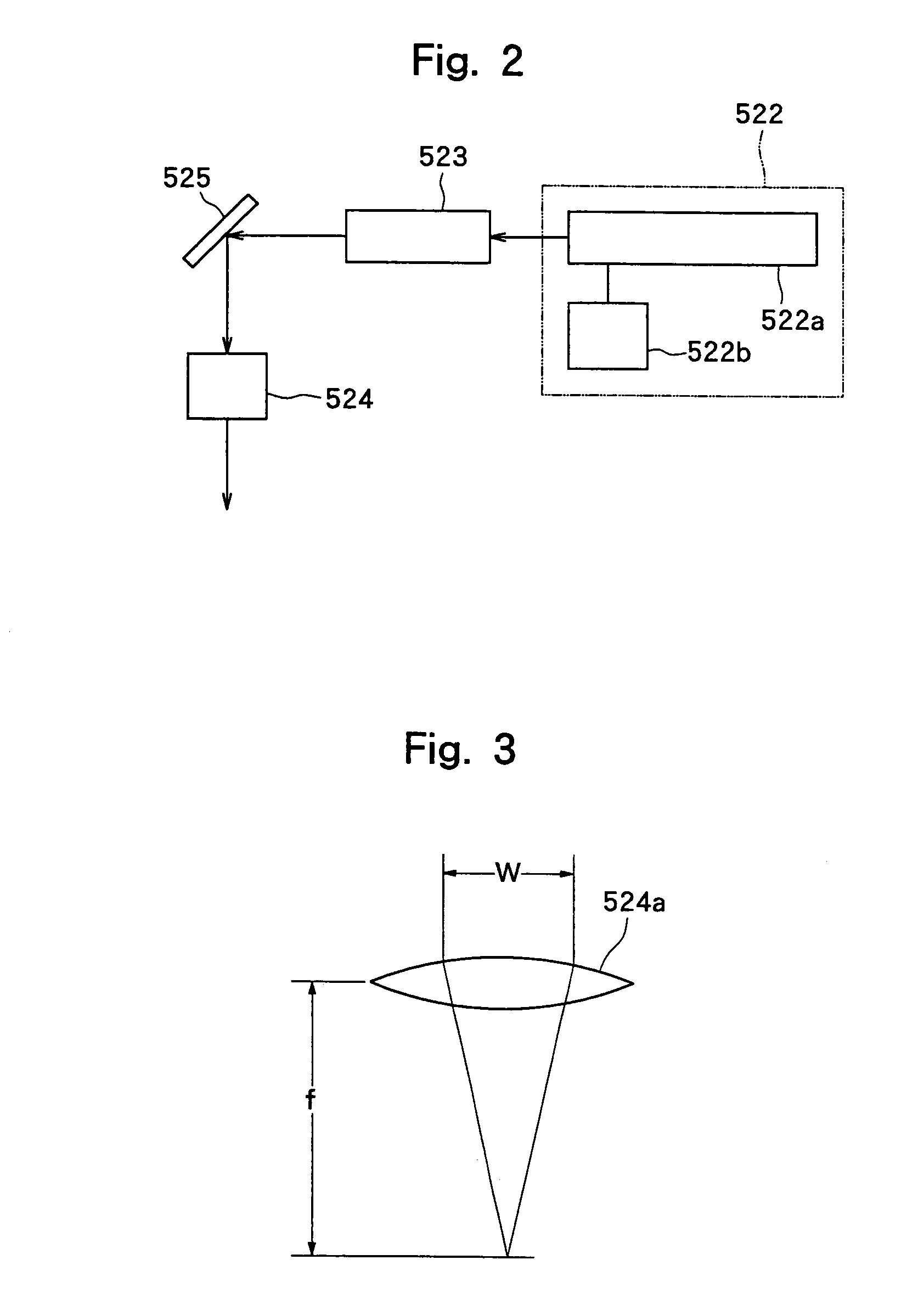
[0024]A laser beam processing method and a laser beam machine according to preferred embodiments of the present invention will be described in detail hereinunder with reference to the accompanying drawings.

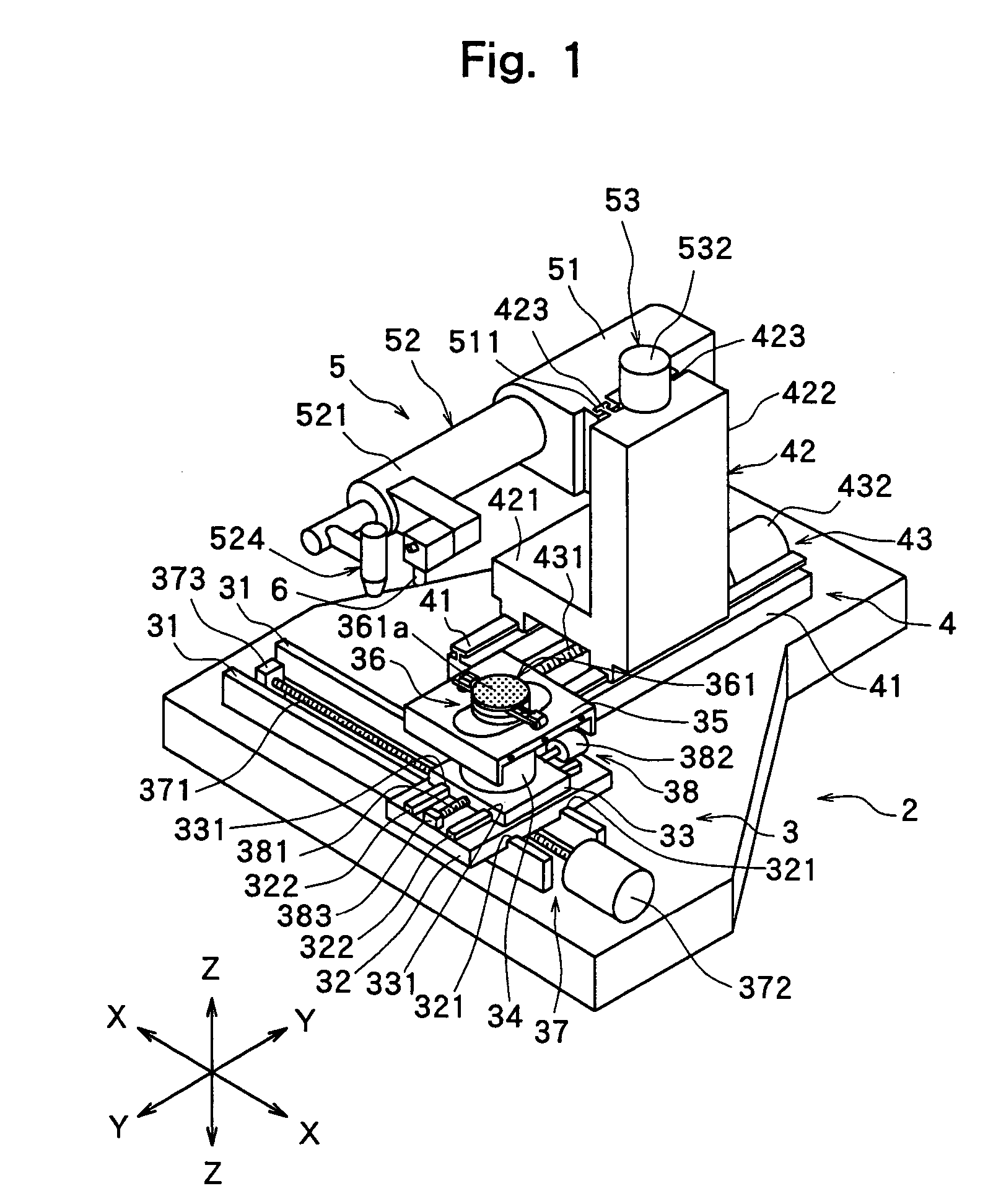
[0025]FIG. 1 is a perspective view of the laser beam machine constituted according to the present invention. The laser beam machine shown in FIG. 1 comprises a stationary base 2, a chuck table mechanism 3, which is mounted on the stationary base 2 in such a manner that it can move in a processing-feed direction indicated by an arrow X and holds a workpiece, a laser beam application unit support mechanism 4 mounted on the stationary base 2 in such a manner that it can move in an indexing-feed direction indicated by an arrow Y perpendicular to the direction indicated by the arrow X, and a laser beam application unit 5 mounted on the laser beam application unit support mechanism 4 in such a manner that it can move in a direction indicated by an arrow Z.

[0026]The above chuck table mec...


PUM

PropertyMeasurementUnit
diameteraaaaaaaaaa
diameteraaaaaaaaaa
widthaaaaaaaaaa

Abstract

A laser beam processing method comprising the step of processing-feeding a wafer having devices which are formed in a large number of areas sectioned by streets arranged in a lattice pattern on the front surface while a laser beam capable of passing through the wafer is applied to the wafer to form deteriorated layers along the streets in the inside of the wafer, wherein the laser beam is applied at a predetermined angle toward a direction intersecting at right angles to the processing-feed direction relative to a direction perpendicular to the laser beam applied surface of the wafer.

Description

CROSS-REFERENCE TO RELATED APPLICATION[0001]The present application contains subject matter related to the Japanese patent application JP 2003-334951, filed in the Japanese Patent Office on Sep. 26, 2003, the entire contents of which being incorporated herein by reference.FIELD OF THE INVENTION[0002]The present invention relates to a laser beam processing method and a laser beam machine for applying a laser capable of passing through a wafer having devices which are formed in a plurality of areas sectioned by dividing lines called “streets” formed in a lattice pattern on the front surface thereof, to the wafer along the streets, to form deteriorated layers in the inside of the wafer.DESCRIPTION OF THE PRIOR ART[0003]In the production process of a semiconductor device, a plurality of areas are sectioned by streets arranged in a lattice pattern on the front surface of a substantially disk-like semiconductor wafer and a circuit (device) such as IC, LSI or the like is formed in each of ...

Claims


Application Information

Patent Timeline
Patent Type & Authority Patents(United States)
IPC IPC(8): H01L21/301B23K26/16H01L21/46H01L21/78B23K26/38B23K26/40B23K101/40H01L21/304
CPCB23K26/08B23K26/0807B23K26/4075H01L21/3043B23K2201/40B23K26/082B23K26/40B23K2101/40B23K2103/50
Inventor NAGAI, YUSUKEKOBAYASHI, SATOSHI
Owner DISCO CORP
Why Eureka
Try Eureka