Memory cell having enhanced high-K dielectric

a memory cell and dielectric layer technology, applied in the direction of basic electric elements, semiconductor devices, electrical equipment, etc., can solve the problems of reducing the threshold voltage of the device, reducing the net positive charge in the charge storage layer, and affecting the performance of the device, so as to reduce the leakage current, and the barrier height is sufficient

Active Publication Date: 2008-04-29
SPANSION LLC
View PDF33 Cites 91 Cited by
  • Summary
  • Abstract
  • Description
  • Claims
  • Application Information

AI Technical Summary

Benefits of technology

[0009]According to one implementation consistent with principles of the invention, a memory device is provided that includes a gate dielectric formed on a substrate, a charge storage layer formed on the gate dielectric, an intergate dielectric formed on the charge storage layer, the intergate dielectric having a sufficient K value to prevent back gate injection and sufficient barrier height to reduce leakage current, and a control gate formed above the intergate dielectric.
[0010]According to another implementation consistent with principles of the invention, an integrated circuit is provided that includes an array of memory cells formed on a semiconductor substrate. Each of the memory cells includes a gate dielectric formed on the substrate, a charge storage layer formed on the gate dielectric, an intergate dielectric formed on the charge storage layer, the intergate dielectric having a sufficient K value to prevent back gate injection and sufficient barrier height to reduce leakage current, and a control gate formed above the intergate dielectric.
[0011]According to yet another implementation consistent with principles of the invention, a method is provided for fabricating a non-volatile memory device. The method includes forming at least one dielectric layer on a semiconductor substrate; forming a charge storage layer on the at least one dielectric layer; forming at least one intergate dielectric layer on the charge storage layer; and forming a control gate on the at least one intergate dielectric layer, wherein the intergate dielectric layer has a sufficient K value to prevent back gate injection and sufficient barrier height to reduce current leakage.

Problems solved by technology

This causes a net positive charge in the charge storage layer and reduces the threshold voltage of the device.
Unfortunately, thin SiO2 layers may break down when subjected to an electric field, particularly SiO2 layers having thicknesses less than 50 Å (5 nm) thick.
In this manner, a leakage current may undesirably form between the control gate and the charge storage layer, adversely affecting the operability of the device.
This exponential increase in the SiO2 layer leakage current can significantly affect the operation of semiconductor devices, particularly with regard to reliability and lifetime.

Method used


Image

  • Memory cell having enhanced high-K dielectric
  • Memory cell having enhanced high-K dielectric
  • Memory cell having enhanced high-K dielectric

Examples


Embodiment Construction

[0018]The following detailed description of the invention refers to the accompanying drawings. Also, the following detailed description does not limit the invention. Instead, the scope of the invention is defined by the appended claims and equivalents.

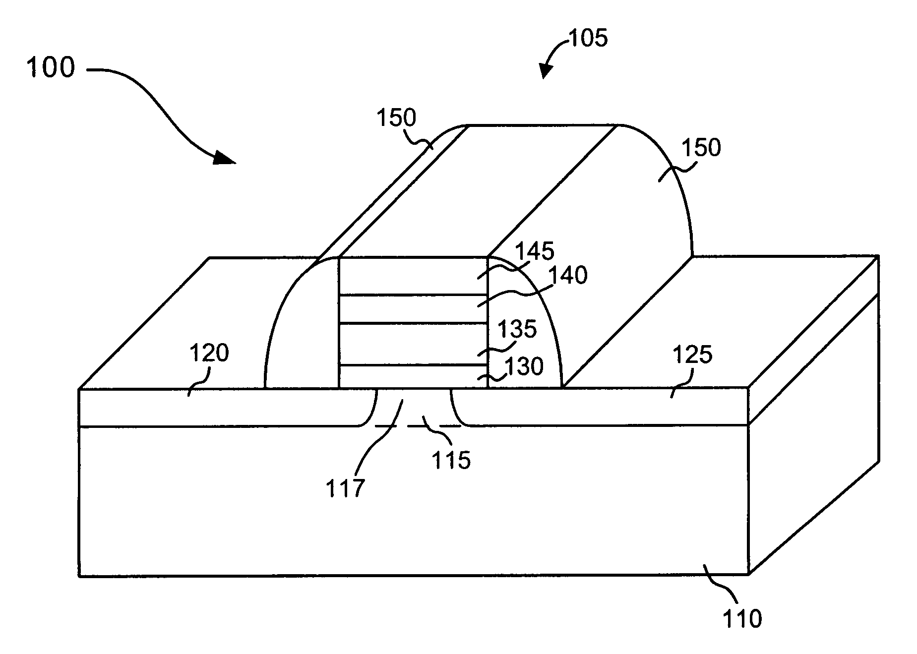
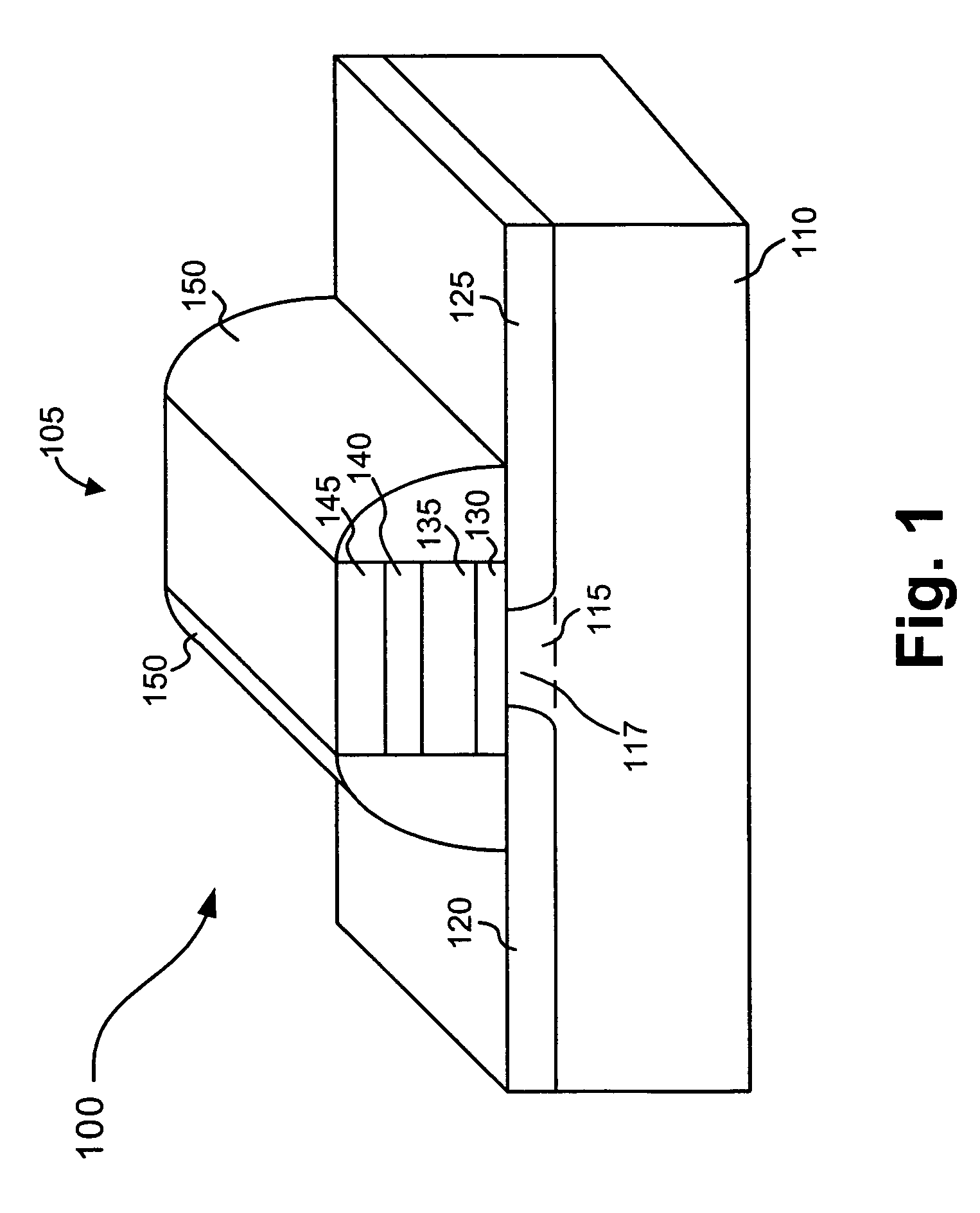
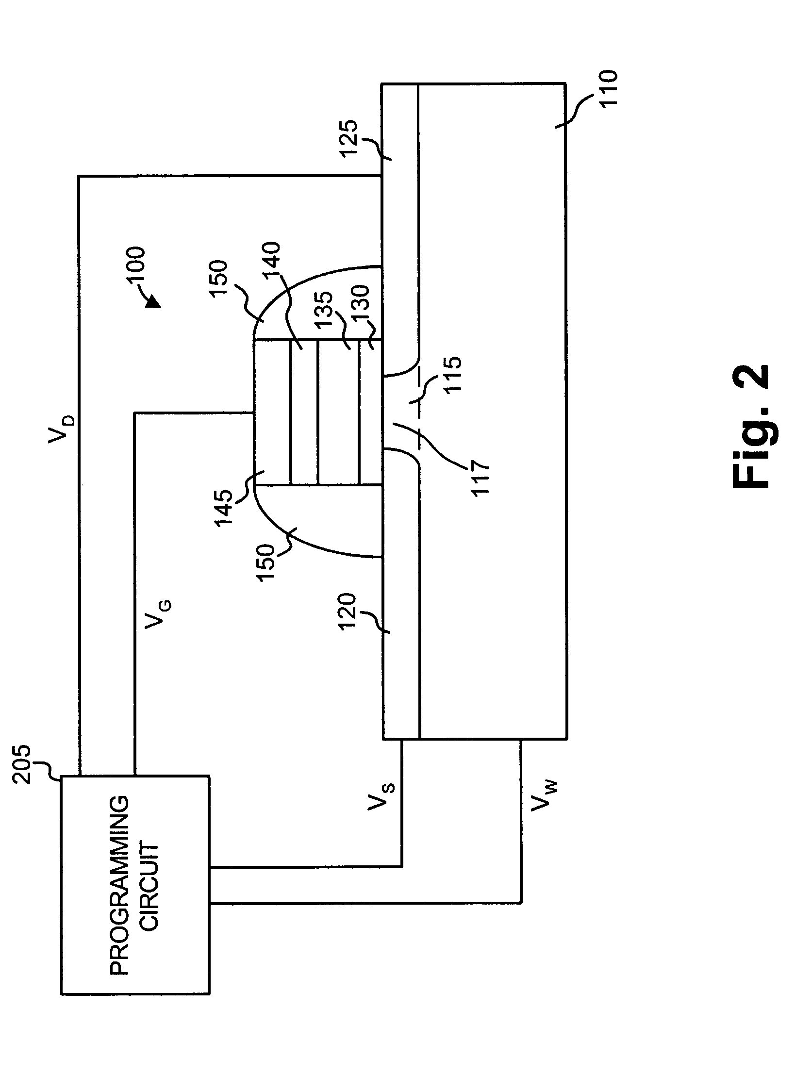
[0019]Techniques described below relate to a semiconductor memory device, a method of using the semiconductor memory device, and a method of making the semiconductor memory device. The semiconductor memory device may include an intergate dielectric layer including a high-K dielectric material interposed between the charge storage layer and the control gate. With this intergate high-K dielectric in place, the memory device may be programmed with hot electron injection and erased using Fowler-Nordheim (F-N) tunneling. Although generally described herein as a single layer, it should be understood by those skilled in the art that the intergate dielectric layer of high-K dielectric material may include one or more layers of the same or diff...


PUM


Abstract

A semiconductor memory device may include an intergate dielectric layer of a high-K, high barrier height dielectric material interposed between a charge storage layer and a control gate. With this intergate high-K, high barrier height dielectric in place, the memory device may be efficiently erased using Fowler-Nordheim tunneling.

Description

TECHNICAL FIELD[0001]Techniques described herein relate generally to non-volatile memory (NVM) devices, and more specifically, to non-volatile memory devices having an enhanced dielectric layer.BACKGROUND ART[0002]Conventional semiconductor memory devices may use a memory structure characterized by a vertical stack of a tunnel oxide (SiO2), a polysilicon floating gate over the tunnel oxide, an intergate dielectric over the floating gate, and a control gate over the interlayer dielectric. The vertical stack may be formed on a crystalline silicon substrate. The substrate may include a channel region positioned below the vertical stack and source and drain on opposing sides of the channel region.[0003]One particular type of flash memory cell structure is characterized by a vertical stack that includes an insulating oxide tunnel layer, a charge trapping nitride dielectric layer, an insulating top oxide layer, and a polysilicon control gate, all positioned on top of a crystalline silicon...

Claims


Application Information

Patent Timeline
Patent Type & Authority Patents(United States)
IPC IPC(8): H01L29/792
CPCH01L29/513H01L29/792
Inventor JEON, JOONGZHENG, WEIRANDOLPH, MARKDING, MENGSHIRAIWA, HIDEHIKO
Owner SPANSION LLC
Why Eureka
Try Eureka