Low-power, low-jitter, fractional-N all-digital phase-locked loop (PLL)

a phase-locked loop, fractional-n technology, applied in the direction of angle demodulation by phase difference detection, automatic control of pulses, electrical apparatus, etc., can solve the problems of limiting the output frequency to the output frequency is limited to be an integer multiple of the input frequency, and the problem of system-on-chip problems

Active Publication Date: 2008-04-29
ATMEL CORP
View PDF5 Cites 34 Cited by
  • Summary
  • Abstract
  • Description
  • Claims
  • Application Information

AI Technical Summary

Problems solved by technology

Generally, one of the main limitations of a conventional PLL 100 is that the output frequency is limited to be an integer multiple of the input frequency.
This can be quite problematic for system-on-chip (SOC) and software defined radios (SDRs) where multiple standards and multiple applications are integrated on one chip.
If an integer PLL 100 is used, then multiple external crystal oscillators 114 must typically be used, which tends to increase the board area, cost, and generally limits the ability to integrate higher level functions on one board.
The main disadvantage of a conventional fractional-N PLL 150 is that the choice of N and N+1 division ratios is chosen in a periodic fashion.
First, the sigma-delta quantization noise is typically still too high.
However, in most clock generator applications, a compact ring oscillator-based VCO is used, which has a notoriously high-phase noise.
In these types of applications, the minimum total integrated phase noise, or jitter, produced by the PLL 200 is generally limited by equally balancing the jitter due to the sigma-delta quantization noise and the jitter due to the VCO phase noise.
Since any mismatch or non-linearity in the PFD 111 can result in unequal step sizes or non-uniform sampling of the output of the divider 113, this can result in degradation in the high-pass noise shaping function of the sigma-delta modulator 202, which may lead to excessive in-band phase noise, and hence degradation of the performance of the PLL 200.
Third, analog PLL design is generally prone to various disadvantages.
One disadvantage of an analog implementation of a PLL 100, 150, 200 is large die area for the LF capacitors (which can occupy as much as 50% of the total area of the PLL 100, 150, 200).
A second disadvantage is significant noise coupling through the substrate for a SOC design can seriously degrade the performance of the PLL 100, 150, 200.
A third disadvantage is large undesired reference tones in the oscillator signal can develop due to gate leakage in the LF capacitors.
Gate leakage generally increases exponentially with the reduction in oxide thickness and is thus more problematic as integrated circuit (IC) technology scales smaller.
However, a major challenge for a digital fractional-N PLL design is obtaining a wide closed loop bandwidth while minimizing the spurious fractional-N tones or sigma-delta quantization noise.
However, this method is generally performed in the analog domain and may severely limit the achievable performance and generally impractically increases the die area.
Additionally, the method may further comprises providing a fine phase error; and counting coarse phase errors in steps of VCO periods or multiples thereof.

Method used


Image

  • Low-power, low-jitter, fractional-N all-digital phase-locked loop (PLL)
  • Low-power, low-jitter, fractional-N all-digital phase-locked loop (PLL)
  • Low-power, low-jitter, fractional-N all-digital phase-locked loop (PLL)

Examples


Embodiment Construction

[0036]The embodiments herein and the various features and advantageous details thereof are explained more fully with reference to the non-limiting embodiments that are illustrated in the accompanying drawings and detailed in the following description. Descriptions of well-known components and processing techniques are omitted so as to not unnecessarily obscure the embodiments herein. The examples used herein are intended merely to facilitate an understanding of ways in which the embodiments herein may be practiced and to further enable those of skill in the art to practice the embodiments herein. Accordingly, the examples should not be construed as limiting the scope of the embodiments herein.

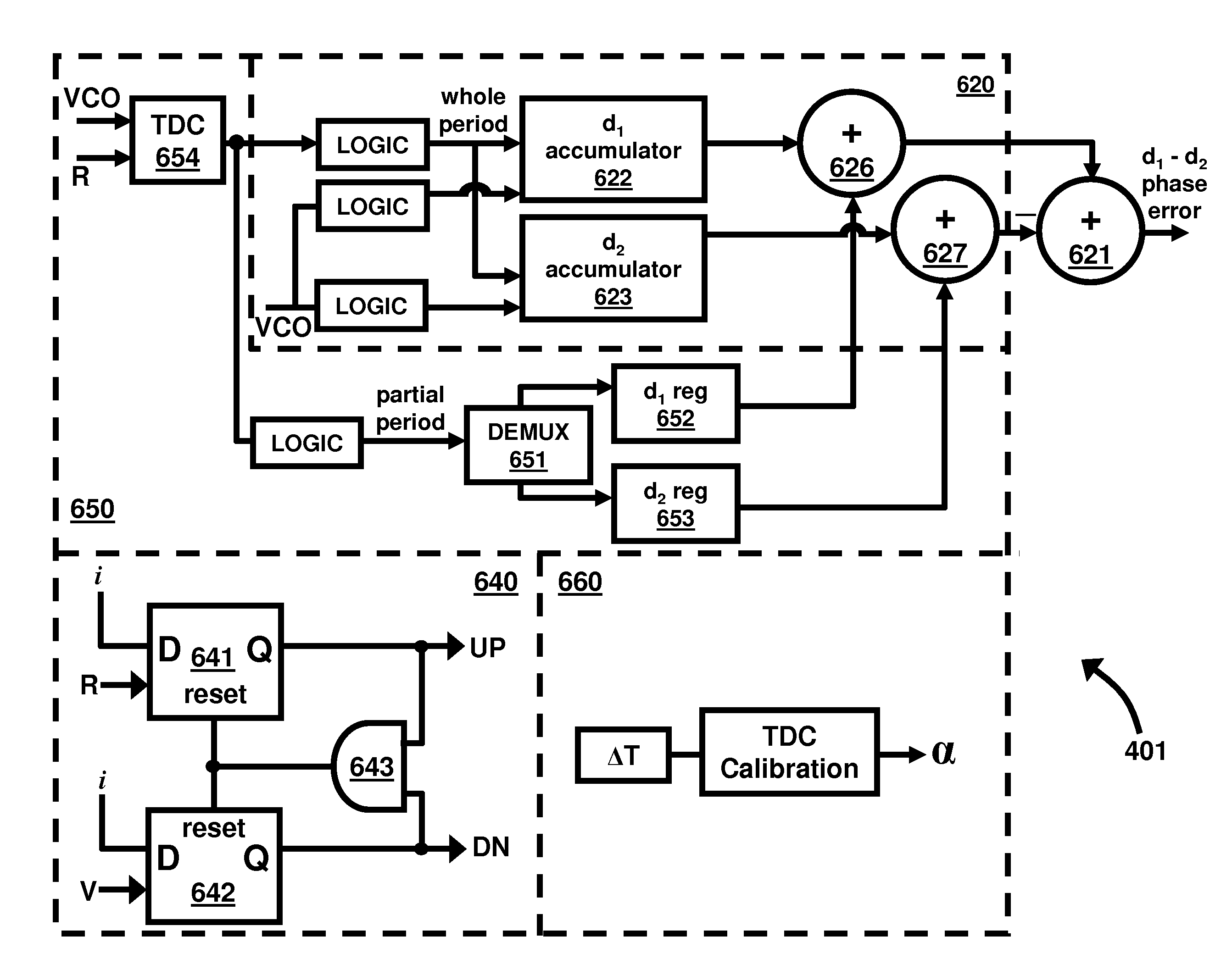
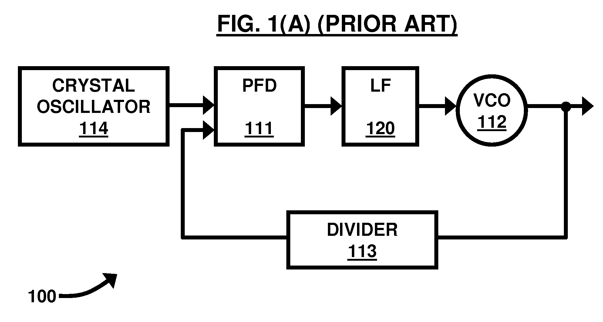
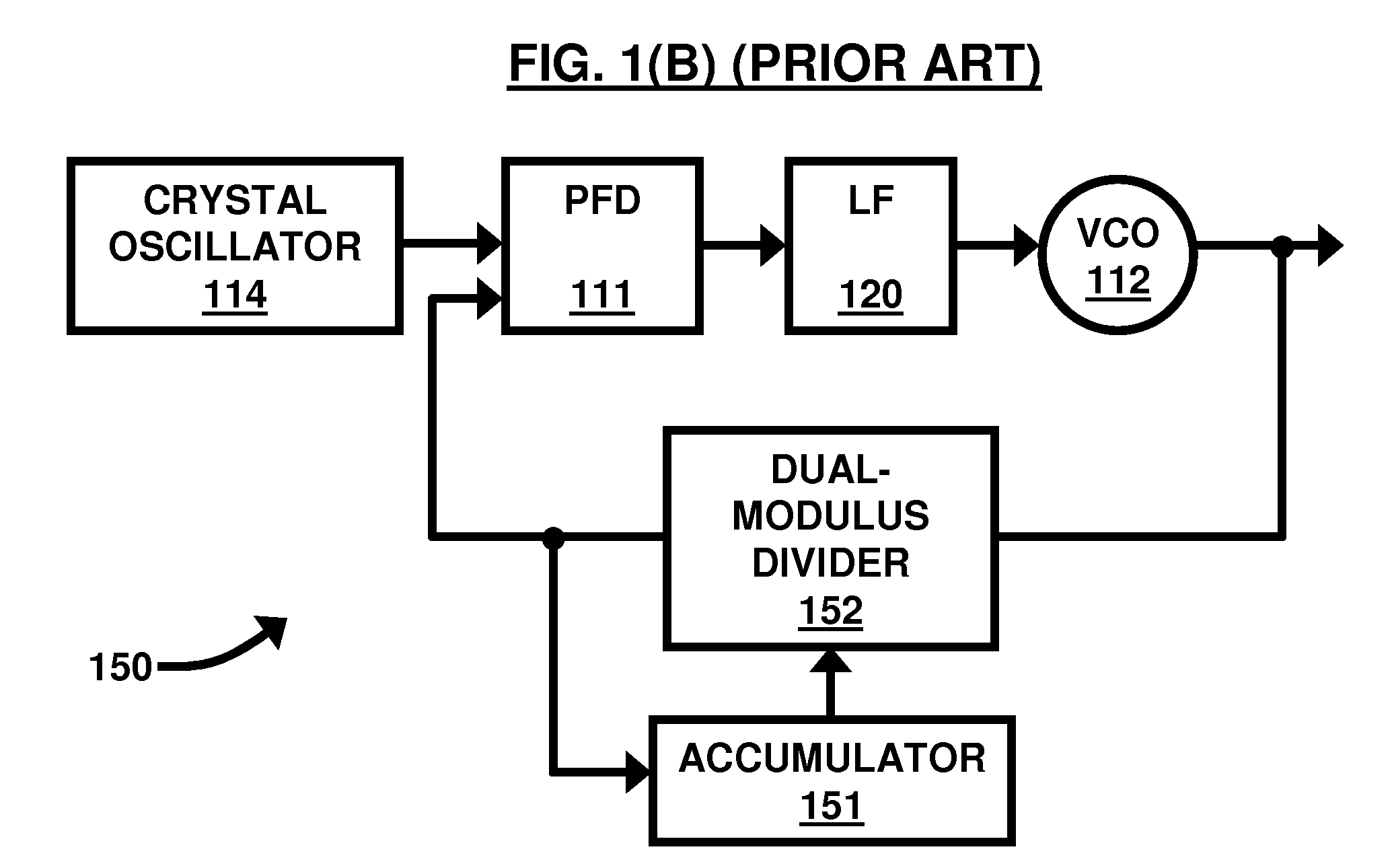
[0037]As previously mentioned, there is a limitation to the minimum jitter achieved by a sigma-delta PLL which is dictated by balancing the jitter contribution of the sigma-delta quantization noise and the jitter contribution of the VCO phase noise. This minimum jitter is still quite high for m...


PUM


Abstract

A method for synthesizing frequencies with a low-jitter an all-digital fractional-N phase-locked loop (PLL) electronic circuit adapted to synthesize frequencies with low-jitter, wherein the electronic circuit comprises a digital phase-frequency detector (DPFD) operatively connected to a digital loop filter (DLF), wherein the DPFD adapted to receive a reference signal and a feedback signal; compare a phase and frequency of the reference and feedback signals to determine a phase and frequency error between the reference and feedback signals; and provide a DPFD output comprising a multi-bit output; wherein the DLF is adapted to receive and filter the DPFD output and provide a DLF output, and wherein the DLF output is updated at each reference period.

Description

BACKGROUND[0001]1. Technical Field[0002]The embodiments herein generally relate to electronics circuits, and, more particularly, to a digital phase-locked loop (PLL) electronic circuit.[0003]2. Description of the Related Art[0004]Phase-locked loops (PLLs) are an integral part of many electronic circuits and are particularly important in communication circuits. For example, digital systems use clock signals to trigger synchronous circuits (e.g., flip-flops). Transmitter and receiver systems use local oscillator (LO) signals for frequency up-conversion and down-conversion, respectively. A wireless device (e.g., cellular phones) in wireless communication systems typically uses clock signals for digital circuitry and LO signals for transmitter and receiver circuitry. Clock and LO signals are often generated with phase-locked loops.[0005]FIG. 1(A) shows a conventional integer PLL 100, which generally consists of a crystal oscillator 114, a phase frequency detector (PFD)111, a loop filter...

Claims


Application Information

Patent Timeline
Patent Type & Authority Patents(United States)
IPC IPC(8): H03L7/00
CPCH03L7/085H03L7/187H03L7/1976
Inventor FAHIM, AMR
Owner ATMEL CORP
Why Eureka
Try Eureka