Method for plasma etching to manufacture electrical devices having circuit protection

a technology of circuit protection and plasma etching, which is applied in the direction of etching metal masks, positive temperature coefficient thermistors, printed element electric connection formation, etc., can solve the problems of preventing good electrical connection, causing resin smear on the substrate, and using expensive and environmentally harsh chemical processes. , to achieve the effect of improving the method of etching a substrate, reducing the cost of etching, and improving the manufacturing process

Inactive Publication Date: 2008-05-06
LITTELFUSE INC
View PDF13 Cites 17 Cited by
  • Summary
  • Abstract
  • Description
  • Claims
  • Application Information

AI Technical Summary

Benefits of technology

[0015]It is therefore an advantage of the present invention to provide an improved process for manufacturing products including circuit protection.
[0016]Another advantage of the present invention is to provide an improved method for making through-holes in devices.
[0017]Yet another advantage of the present invention is to provide a method of making smaller fuses.
[0018]An

Problems solved by technology

Of course, given the sensitive nature of such devices, it is necessary to protect these printed circuit boards against electrical overloads and overvoltage.
However, drilling processes typically generate a resin smear on the

Method used


Image

  • Method for plasma etching to manufacture electrical devices having circuit protection
  • Method for plasma etching to manufacture electrical devices having circuit protection
  • Method for plasma etching to manufacture electrical devices having circuit protection

Examples


Embodiment Construction

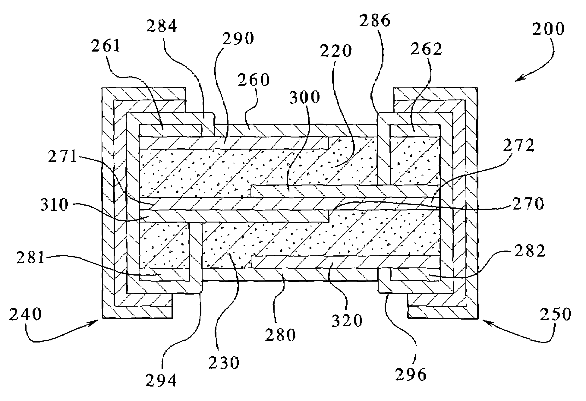
[0044]The present invention provides methods for manufacturing devices having circuit protection and devices so manufactured. It should be appreciated that a variety of such devices can be manufactured.

[0045]An embodiment of the present invention is shown in FIG. 11. The thin film, surface-mounted electrical protection component is a subminiature device used in a surface mount configuration on a PC board. One such electrical protection component is a fuse. A fuse common in the art is an “A” case fuse. The standard industry size for “A” case fuses is 120 mils long by 60 mils wide. The “A” case fuse is also designated as a 1206 fuse. In addition, the present invention includes even smaller sized fuses, which are compatible with standard sized surface mountable devices. The present invention can be used with all other standard sizes of such surface mountable device sizes, such as 1210, 0805, 0603 and 0402 fuses, as well as non-standard sizes. The present invention can be used with a va...


PUM

PropertyMeasurementUnit
Timeaaaaaaaaaa
Currentaaaaaaaaaa
Areaaaaaaaaaaa

Abstract

Methods of manufacturing a variety of circuit protection devices are provided as well as devices so manufactured. In an embodiment, a surface mount electrical device having a substrate and a pair of conductive electrodes connected to an electrical protection component for sensing current or voltage is provided. The method includes the steps of: (i) providing a substrate having a first surface and a second surface; creating a first and second aperture, plasma etching a through-hole, slot or bore through the substrate; (ii) depositing a conductive material on the substrate and through the apertures to form the electrodes, wherein the conductive material extends through the apertures and on the first and second surfaces of the substrate, respectively; and (iii) depositing the electrical protection component on the first surface of the substrate to electrically connect the electrodes.

Description

BACKGROUND OF THE INVENTION[0001]The present invention relates generally to electrical devices. More specifically, the present invention relates to methods of manufacturing devices having circuit protection.[0002]Printed circuit (PC) boards have found increasing application in electrical and electronic equipment of all kinds. For example, an onslaught of wireless communications has created the need for large quantities of low cost, high performance circuit boards. In addition to increasing the performance of such devices, manufacturers strive to reduce the physical size of the devices.[0003]Of course, given the sensitive nature of such devices, it is necessary to protect these printed circuit boards against electrical overloads and overvoltage. This protection may be provided by temperature, voltage or current protection components that are physically secured to the PC board. For example, such protection can be provided by positive temperature coefficient (PTC) elements, electrostat...

Claims


Application Information

Patent Timeline
IPC IPC(8): H01H69/02H01C1/14H01C7/02H01C17/00H01C17/28H05K3/00H05K3/40H05K3/42
CPCH01C1/1406H01C17/006H01C17/28H01H69/022H05K3/403H01C7/02Y10T29/49107H01H2085/0414H05K3/0041H05K3/0052H05K3/428H05K2201/09181H05K2203/0554Y10T29/49082Y10T29/4913Y10T29/49126Y10T29/49165Y10T29/49155
Inventor RYBKA, MATTHEWRESTIS, THOMAS
Owner LITTELFUSE INC
Why Eureka
Try Eureka