

Method for fabricating a resistive memory
a resistive memory and manufacturing method technology, applied in semiconductor/solid-state device manufacturing, basic electric elements, electric apparatus, etc., can solve the problems of inability to solve in an optimal way, the charge quantity which can be held in a cell is also becoming ever smaller, and the memory cells based on capacitive charging no longer operate satisfactorily
- Summary
- Abstract
- Description
- Claims
- Application Information
AI Technical Summary
Benefits of technology
Problems solved by technology
Method used
Image

Examples
Embodiment Construction
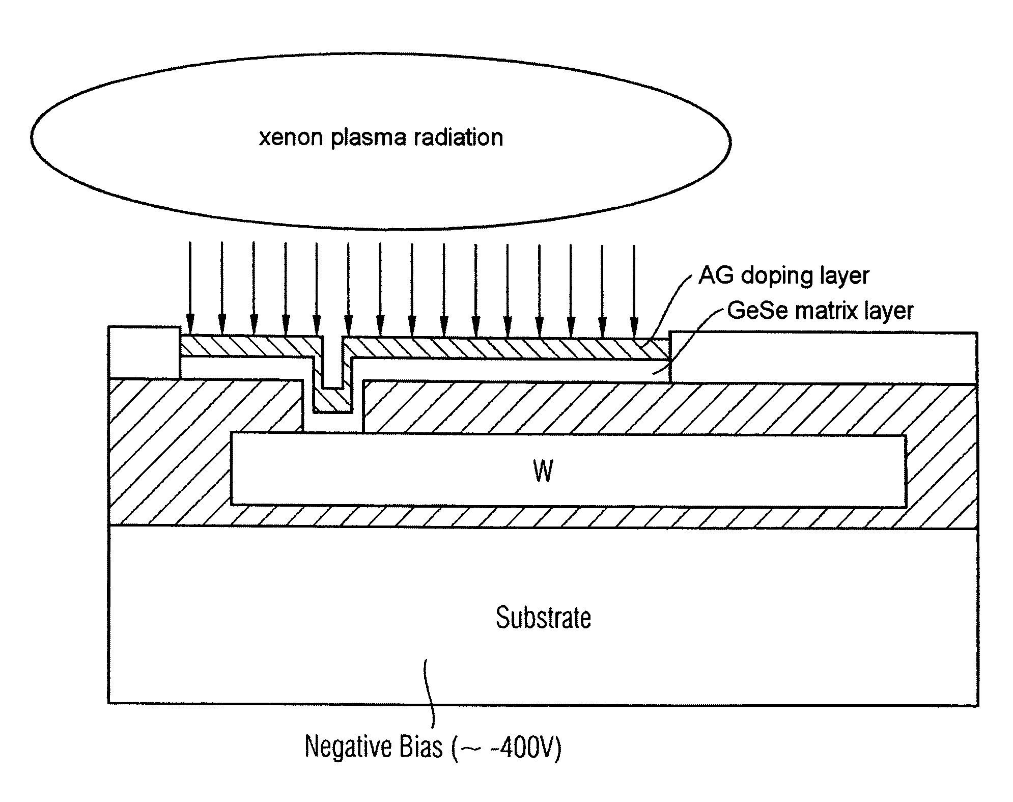
[0023]The invention provides a method for fabricating a resistively switching memory cell, where the method includes depositing a first electrode, applying a layer of a chalcogenide compound to the first electrode, applying a metallic doping layer of silver or copper in a first noble gas plasma to the layer of the deposited chalcogenide compound, and applying a silver-copper diffusion from the applied metallic doping layer into the layer of the chalcogenide compound in a second noble gas plasma and via a back-sputtering process.
[0024]An important feature of the invention is the elimination of the conventional separate photodiffusion step by UV exposure of the Ag layer. This is made possible by the sputtered-on Ag doping layer being made to diffuse into, e.g., a GeSe matrix layer by a xenon plasma in the coating installation. Then, the top electrode is deposited without the wafer having to be discharged from the installation or intermediate venting of the installation having to be ca...
PUM
| Property | Measurement | Unit |
|---|---|---|
| voltage | aaaaa | aaaaa |
| voltage | aaaaa | aaaaa |
| voltage | aaaaa | aaaaa |
Abstract
Description
Claims
Application Information