Apparatus and methods for packaging integrated circuit chips with antenna modules providing closed electromagnetic environment for integrated antennas

a technology of integrated circuit chips and antenna modules, applied in the direction of radiating element structural forms, resonant antennas, protective material radiating elements, etc., can solve the problems of increasing the difficulty of manufacturing and assembly of conventional waveguide front-ends, increasing the cost of bulky wave guides, and increasing the difficulty of achieving high-performance systems

Active Publication Date: 2008-05-13
INT BUSINESS MASCH CORP
View PDF7 Cites 153 Cited by
  • Summary
  • Abstract
  • Description
  • Claims
  • Application Information

AI Technical Summary

Benefits of technology

[0008]In general, exemplary embodiments of the invention include apparatus and methods for packaging semiconductor IC (integrated circuit) chips with integrated antennas to construct compact, high-performance radio / wireless communications systems for millimeter wave applications (e.g., voice communication, data communication and radar applications, etc.). More specifically, exemplary embodiments of the invention include apparatus and methods for packaging IC chips together with integrated antenna modules that are designed to provide a closed EM (electromagnetic) environment for antenna radiators, thereby allowing antennas to be designed independent from the packaging technology.

Problems solved by technology

For example, MMW radio communication systems are typically built using expensive and bulky wave guides and / or package-level or board-level micro strip structures that provide electrical connections between semiconductor chips (RF integrated circuits) and between semiconductor chips and transmitter or receiver antennas.
As the operating frequency increases, the manufacture and assembly of conventional waveguide front-ends become more difficult due to high-precision machining and accurate alignment.
With increased integration, however, the ability to achieve high performance systems becomes more problematic, especially at millimeter wave frequencies wherein the structure and EM (electromagnetic) characteristics of the integrated antenna system and package layout will determine the achievable performance of the system.
Indeed, with high-integration designs where integrated antennas are packaged in compact chip packages, the antenna performance will depend on the antenna structure as well as package structures, components and materials that are disposed in proximity to the antenna, which can significantly affect antenna performance.
Further, the characteristics of antenna feed lines that interface active circuitry with the antennas can vary with the package environment and, thus, affect the antenna performance (e.g., impedance mismatch).
Conventional antenna design methods do not allow integrated antennas to be designed independently of the package.
Indeed, with conventional integrated antenna design techniques, an antenna designed for one type of packaging technology may not be applicable for another packaging technology, thereby requiring redesign of the antenna.

Method used


Image

  • Apparatus and methods for packaging integrated circuit chips with antenna modules providing closed electromagnetic environment for integrated antennas
  • Apparatus and methods for packaging integrated circuit chips with antenna modules providing closed electromagnetic environment for integrated antennas
  • Apparatus and methods for packaging integrated circuit chips with antenna modules providing closed electromagnetic environment for integrated antennas

Examples


Embodiment Construction

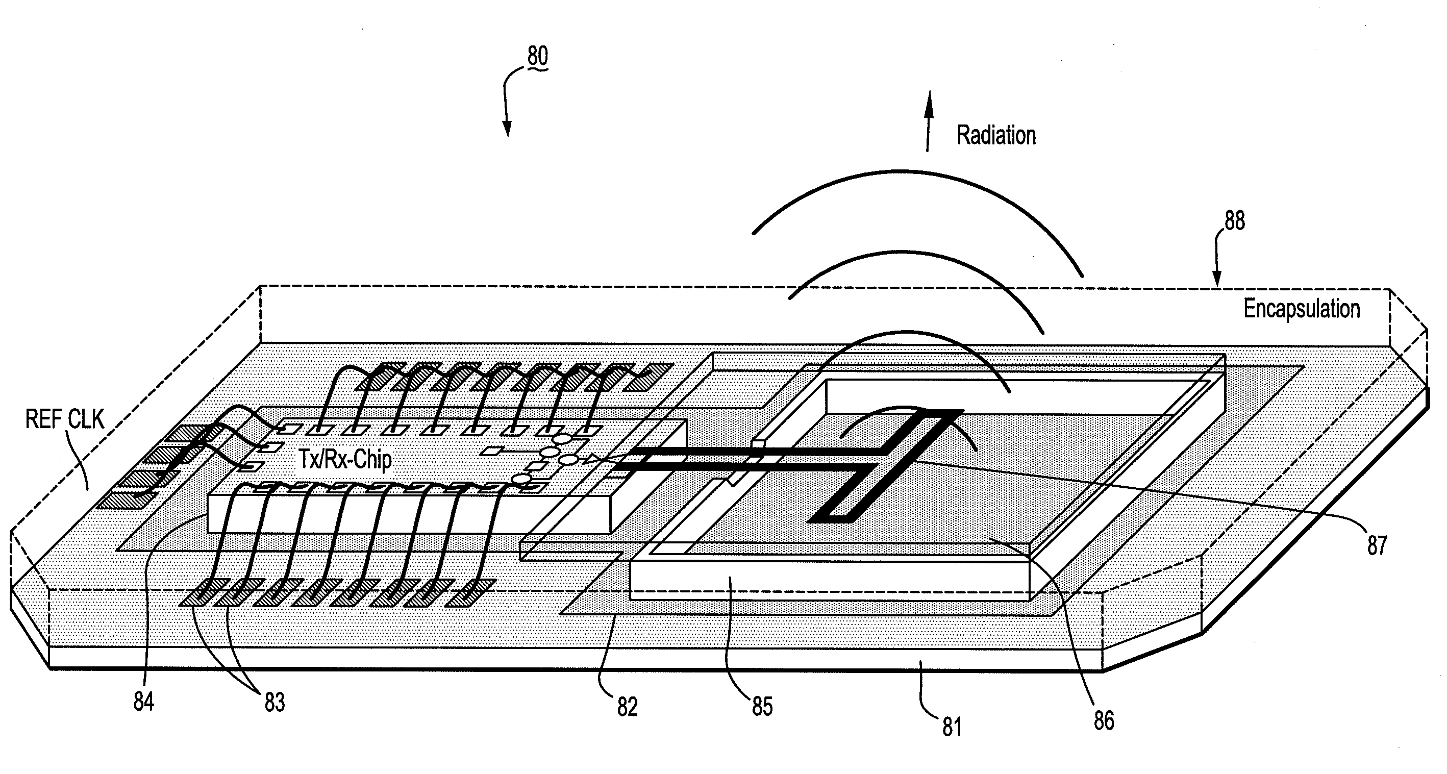
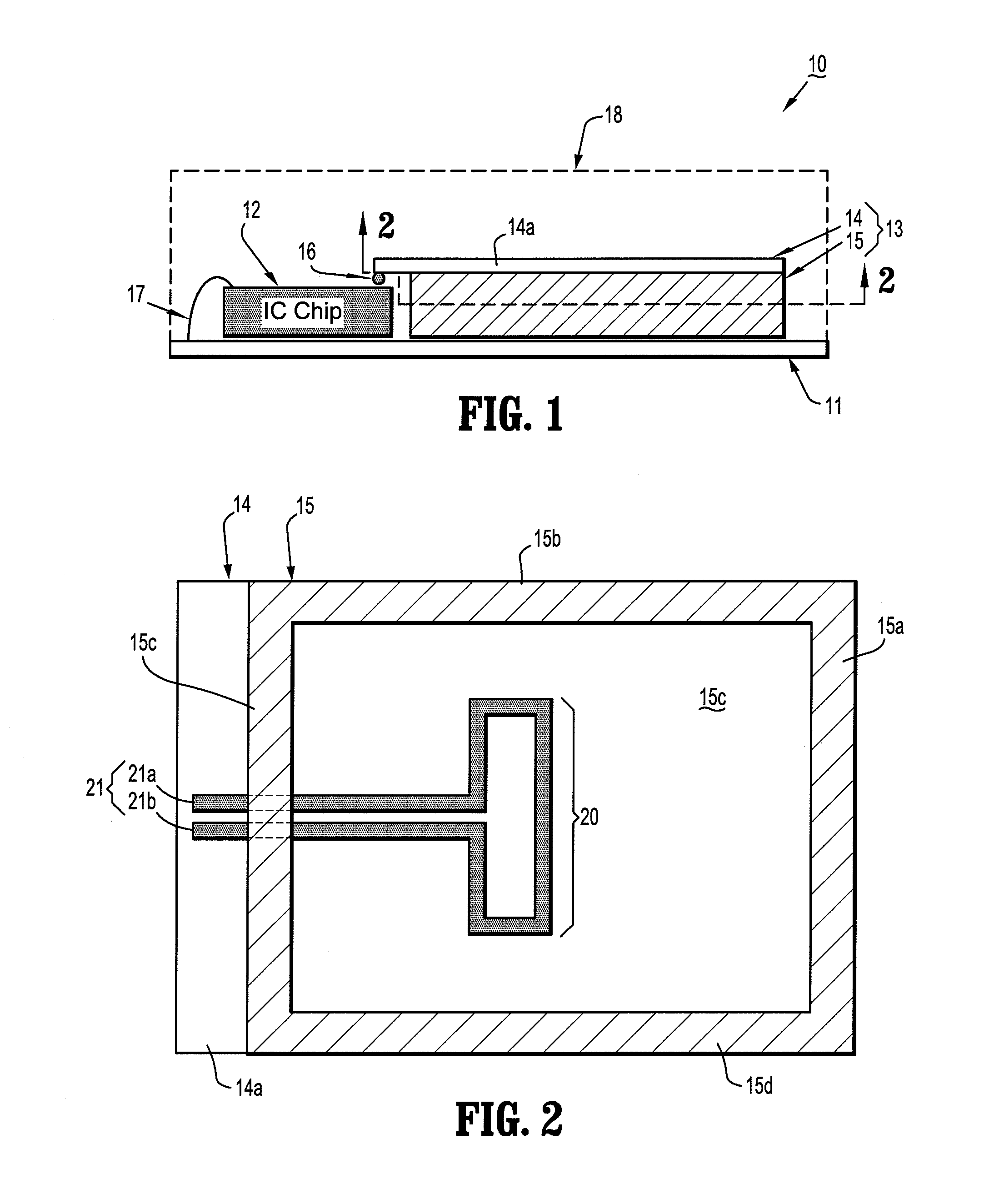
[0023]FIG. 1 schematically illustrates an apparatus for integrally packaging an antenna and IC chip, according to an exemplary embodiment of the present invention. In general, FIG. 1 illustrates an electronic package apparatus (10) comprising a package frame structure (11), an integrated circuit chip (12) backside mounted to the package frame (11), an integrated antenna module (13) mounted to the package frame (11). The package frame can be one of various types of package structures including, but not limited to, package cores, substrates, carriers, die paddles, lead frames, etc., and other package structures that provide functions such as mechanical stability, chip mounting, electrical interface, etc.

[0024]The antenna module (13) comprises an integrated antenna device (14) mounted to an antenna socket structure (15). The integrated antenna device (14) comprises a planar substrate (14a) mounted to the socket structure (15), which has one or more antenna elements and antenna feeds, f...


PUM


Abstract

Apparatus and methods are provided for packaging IC chips together with integrated antenna modules designed to provide a closed EM (electromagnetic) environment for antenna radiators, thereby allowing antennas to be designed independent from the packaging technology.

Description

GOVERNMENT LICENSE RIGHTS[0001]This invention was made with Government support under Contract No. NAS3-03070 awarded by NASA (National Aeronautics and Space Administration). The Government has certain rights in this invention.TECHNICAL FIELD OF THE INVENTION[0002]The present invention generally relates to apparatus and methods for packaging semiconductor IC (integrated circuit) chips with integrated antennas for millimeter wave applications and in particular, to apparatus and methods for packaging IC chips together with integrated antenna modules that are designed to provide a closed EM (electromagnetic) environment for antenna radiators, thereby allowing antennas to be designed independent from the packaging technology.BACKGROUND[0003]Technological innovations in wireless systems and devices have lead to widespread development of wireless network applications for wireless PAN (personal area network), wireless LAN (local area network), wireless WAN (wide area network), cellular netw...

Claims


Application Information

Patent Timeline
Patent Type & Authority Patents(United States)
IPC IPC(8): H01Q1/38
CPCH01Q1/2283H01Q1/38H01Q1/40H01Q7/00H01Q23/00H01L2224/48227H01L2224/48091H01L2924/00014H01L2223/6677H01L2924/3025
Inventor GAUCHER, BRIAN P.GRZYB, JANUSZLIU, DUIXIANPFEIFFER, ULLRICH R.
Owner INT BUSINESS MASCH CORP
Why Eureka
Try Eureka