Thin film transistor array panel

a transistor array and thin film technology, applied in the field of thin film transistor array panels, can solve the problems of disconnection of wires, signal distortion caused by the increase of the resistance of wires and in various parasitic capacitances, and become critical problems, and achieve the effects of low resistance, improved reliability, and easy oxidation

Inactive Publication Date: 2008-05-20
SAMSUNG DISPLAY CO LTD
View PDF17 Cites 6 Cited by
  • Summary
  • Abstract
  • Description
  • Claims
  • Application Information

AI Technical Summary

Benefits of technology

[0008]It is another object of the present invention to provide a thin film transistor array panel with a low resistivity Ag wire having improved reliability.
[0009]These and other objects may be achieved by depositing Ag and an additive easily oxidizable and performing heat treatment to form a wire.

Problems solved by technology

Accordingly, signal distortion due to the increase in the resistance of the wires and in various parasitic capacitances becomes to be a critical problem.
However, silver exhibits poor adhesiveness to a glass substrate or a silicon layer.
The poor adhesiveness frequently causes the defect such as the looseness or detachment of the silver thin films during the subsequent processes such as cleaning, which results in the disconnection of the wire.
Furthermore, silver may be easily damaged by dry etch of the silicon nitride insulating layer.

Method used


Image

  • Thin film transistor array panel
  • Thin film transistor array panel
  • Thin film transistor array panel

Examples


first embodiment

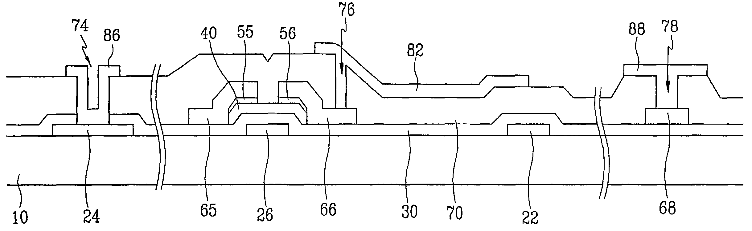
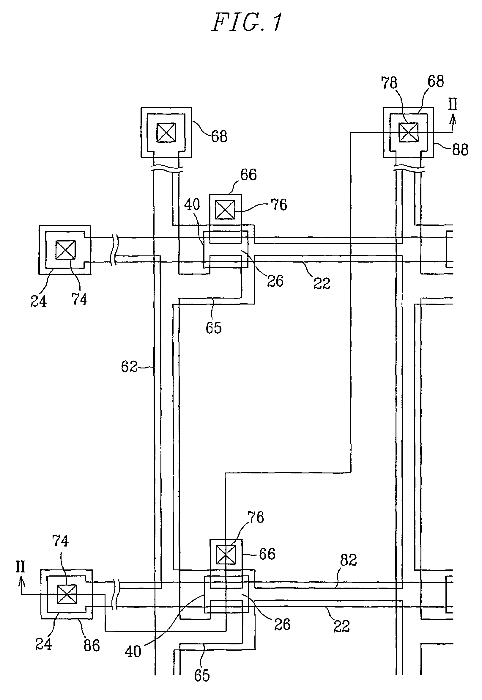
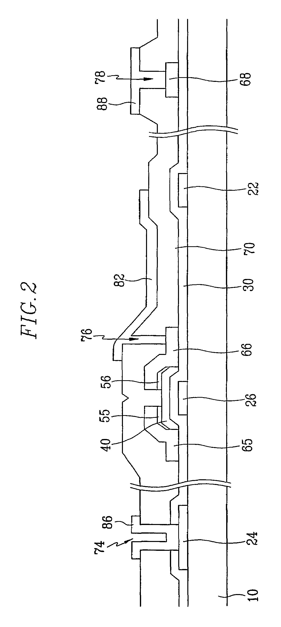
[0066]First, a structure of a TFT array panel for an LCD according to the present invention is described in detail with reference to FIGS. 1 and 2.

[0067]FIG. 1 is a layout view of a TFT array panel for an LCD according to a first embodiment of the present invention, and FIG. 2 is a sectional view of the TFT array panel shown in FIG. 1 taken along the line II-II.

[0068]A gate wire 22, 24 and 26 is formed on an insulating substrate 10. The gate wire 22, 24 and 26 is made of a Ag(Zn) alloy including Ag and additional Zn. A ZnOx layer, which is an oxide of the additive Zn, is formed on the surfaces of the gate wire 22, 24 and 26. The ZnOx portion increases the adhesiveness of the gate wire 22, 24 and 26 to the underlying substrate 10 and protecting the gate wire 22, 24 and 26 from the dry etch using CF4+O2 plasma and the like, in the subsequent steps. The ZnOx is formed by heat treatment of the Ag(Zn) alloy gate wire 22, 24 and 26, which causes the diffusion of Zn to the surfaces thereof...

second embodiment

[0092]FIG. 7 is a layout view of a TFT array panel for an LCD according to the present invention, and FIGS. 8 and 9 are sectional views of the TFT array panel shown FIG. 7 taken along the line VIII-VIII′ and the line IX-IX′, respectively.

[0093]A gate wire 22, 24 and 26 is formed on an insulating substrate 10. Like the first embodiment, the gate wire 22, 24 and 26 is made of Ag(Zn) alloy including Ag and additional Zn. A ZnOx layer, which is an oxide of the additive Zn, is formed on the surfaces of the gate wire 22, 24 and 26. The gate wire includes a plurality of gate lines 22, a plurality of gate pads 24, and a plurality of gate electrodes 26.

[0094]A plurality of storage capacitor lines 28 parallel to the gate lines 22 are formed on the substrate 10. The storage capacitor lines 28 are also made of Ag(Zn) alloy including Ag and additional Zn. A ZnOx layer, which is an oxide of the additive Zn, is formed on the surfaces of the storage capacitor lines 28. The storage capacitor lines 2...

third embodiment

[0148]First, a structure of a TFT array panel for an LCD according to the present invention is described in detail with reference to FIGS. 21 and 22.

[0149]FIG. 21 is a layout view of a TFT array panel for an LCD according to a third embodiment of the present invention, and FIG. 22 is a sectional view of the TFT array panel shown in FIG. 21 taken along the line XXII-XXII′.

[0150]A gate wire 22, 24 and 26 is formed on an insulating substrate 10. The gate wire 22, 24 and 26 is made of a Ag(Zn) alloy including Ag and additional Zn. A ZnOx layer, which is an oxide of the additive Zn, is formed on the surfaces of the gate wire 22, 24 and 26. The gate wire 22, 24 and 26 includes a plurality of scanning signal lines or gate lines 22 extending in the transverse direction, a plurality of gate pads 24 connected to one ends of the gate lines 22 to transmit gate signals from an external device to the gate lines 22, and a plurality of gate electrodes 26 of TFTs, which are parts of the gate lines 2...


PUM

PropertyMeasurementUnit
dielectric constantaaaaaaaaaa
thicknessaaaaaaaaaa
contact resistanceaaaaaaaaaa

Abstract

A thin film transistor array panel includes an insulating substrate, a gate wire formed on the insulating substrate. A gate insulating layer covers the gate wire. A semiconductor pattern is formed on the gate insulating layer. A data wire having source electrodes, drain electrodes and data lines is formed on the gate insulating layer and the semiconductor pattern. A protective layer is formed on the data wire. Pixel electrodes connected to the drain electrode via contact holes are formed on the protective layer. The gate wire and the data wire are made of Ag alloy containing Ag and an additive including at least one selected from Zn, In, Sn and Cr.

Description

BACKGROUND OF THE INVENTION[0001](a) Field of the Invention[0002]The present invention relates to a thin film transistor array panel and a manufacturing method thereof.[0003](b) Description of the Related Art[0004]Generally, a thin film transistor array (“TFT”) panel for a liquid crystal display (“LCD”) or an electro-luminescence (“EL”) display is used as a circuit board for driving the respective pixels in an independent manner. The TFT array panel includes a scanning signal wire or a gate wire transmitting scanning signals, an image signal wire or a data wire transmitting image signals, TFTs connected to the gate and the data wire, pixel electrodes connected to the TFTs, a gate insulating layer covering the gate wire for insulation, and a protective layer covering the TFTs and the data wire for insulation. The TFT includes a gate electrode, which is a part of the gate wire, a semiconductor layer forming a channel, source and drain electrodes, which are parts of the data wire, a ga...

Claims


Application Information

Patent Timeline
Patent Type & Authority Patents(United States)
IPC IPC(8): H01L21/00H01L21/84H01L27/01G02F1/1368H01L21/28H01L21/3205H01L21/336H01L21/77H01L23/52H01L27/12H01L29/423H01L29/45H01L29/49H01L29/786H01L51/50
CPCH01L27/12H01L29/458H01L27/124H01L29/66765H01L29/4908H01L29/786
Inventor LEE, JAE-GABKANG, BONG-JOOCHO, BEOM-SEOKJEONG, CHANG-OH
Owner SAMSUNG DISPLAY CO LTD
Why Eureka
Try Eureka