Semiconductor light emitting device

a technology of light-emitting devices and semiconductors, which is applied in the direction of semiconductor devices, basic electric elements, electrical appliances, etc., can solve the problems of difficult to form p-side electrode films with a smaller contact resistance and a higher reflectivity, and achieve excellent ohmic contact, reduce contact resistance, and increase light extraction efficiency

Active Publication Date: 2008-05-20
ROHM CO LTD
View PDF12 Cites 43 Cited by
  • Summary
  • Abstract
  • Description
  • Claims
  • Application Information

AI Technical Summary

Benefits of technology

[0009]It is an object of the present invention to provide a semiconductor light emitting device of a flip-chip type including a semiconductor light emitting portion bonded to a mounting board in opposed relation and having a light extraction efficiency improved by alleviating restrictions on electrodes disposed adjacent to the mounting board.
[0011]With this arrangement, the transparent electrode is provided on the surface of the second contact layer of the semiconductor light emitting portion, and the metal reflection film is disposed on a back side of the transparent electrode as seen from the side of the semiconductor light emitting portion. Thus, the light emitted from the semiconductor light emitting portion and passing through the transparent electrode is reflected on the metal reflection film toward the semiconductor light emitting portion, thereby providing an excellent light extraction efficiency.
[0012]In addition, there is no need to provide ohmic contact between the metal reflection film and the semiconductor light emitting portion, because the transparent electrode covers substantially the entire surface of the second contact layer. This permits a wider choice of materials for the metal reflection film, making it possible to further increase the light extraction efficiency by selecting a higher reflectivity material or to reduce costs by selecting a less expensive material.
[0018]With this arrangement, the transparent insulation film is disposed between the transparent electrode and the metal reflection film, so that the reflection of the light from the semiconductor light emitting portion mostly occurs in an interface between the transparent insulation film and the metal reflection film. Since virtually no light absorption occurs in an insulator / metal interface, the light extraction efficiency can be further improved.
[0023]The transparent electrode preferably comprises a Zn1-xMgxO (wherein 0≦x<1) film. Zn1-xMgxO (wherein 0≦x<1 and, when x=0, ZnO) provides excellent ohmic contact with a GaN semiconductor layer, and has a transmittance of not lower than 80% with respect to light of a wavelength range of 370 nm to 1000 nm. This makes it possible to reduce the contact resistance and further increase the efficiency of light extraction through the front electrode.

Problems solved by technology

However, it is necessary to provide the P-side and N-side electrodes on the InGaN semiconductor light emitting portion and route wires from the electrodes, because the sapphire substrate is insulative.
Therefore, light from the InGaN semiconductor light emitting portion is blocked by the electrodes and the like, so that the light extraction efficiency is low.
This imposes heavy restrictions on device production, making it difficult to form a P-side electrode film having a smaller contact resistance and a higher reflectivity.Patent Document 1: Japanese Patent Publication No.Patent Document 2: Japanese Unexamined Patent Publication No. 2003-224297

Method used


Image

  • Semiconductor light emitting device
  • Semiconductor light emitting device
  • Semiconductor light emitting device

Examples


Embodiment Construction

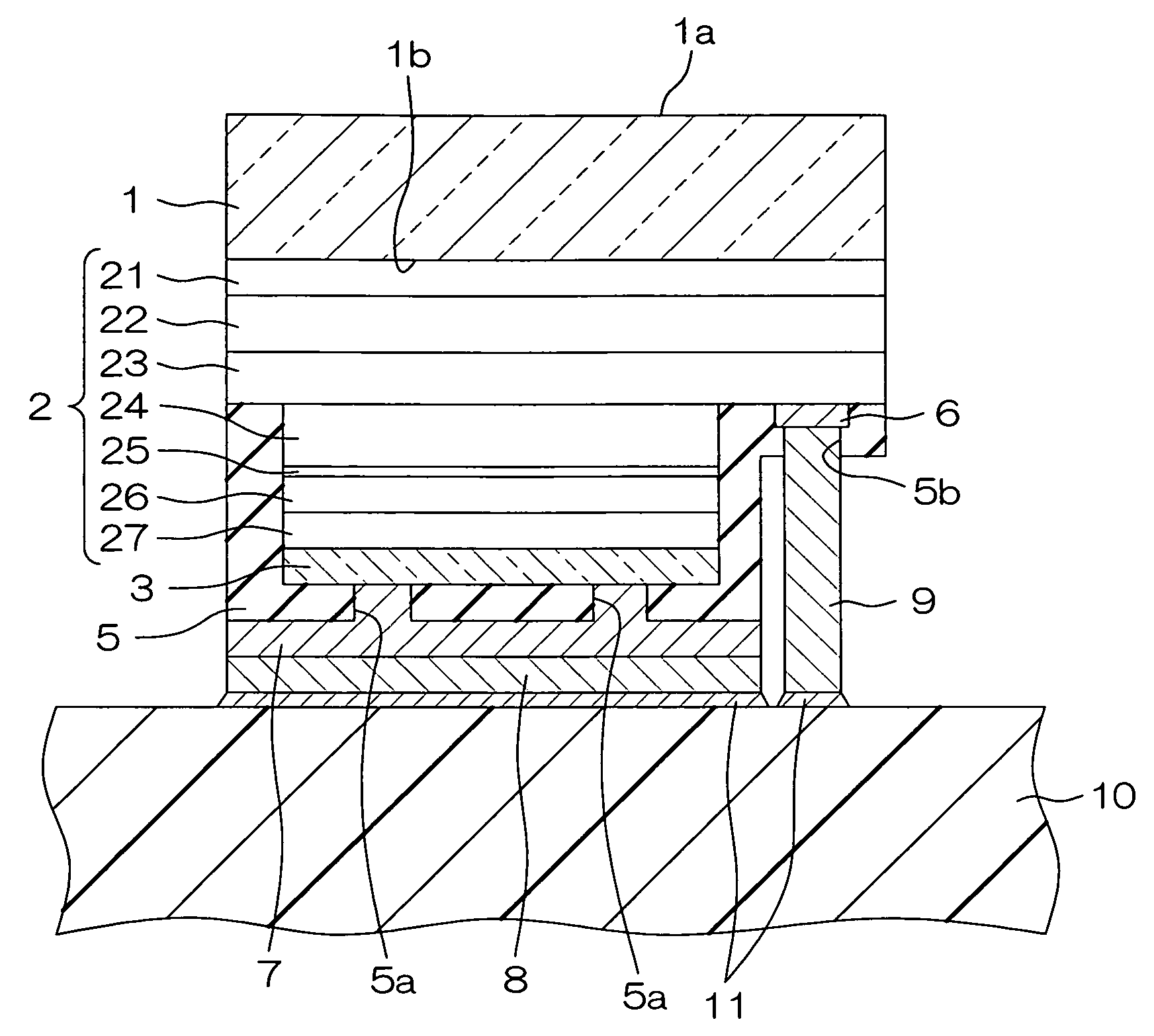
[0032]FIG. 1 is a sectional view schematically illustrating the construction of a light emitting diode element according to one embodiment of the present invention. The light emitting diode element is of a flip-chip type, and includes a sapphire substrate 1 as a transparent substrate, an InGaN semiconductor light emitting portion 2 provided on the sapphire substrate 1, and a P-side transparent electrode 3 covering a surface of the InGaN semiconductor light emitting portion 2 opposite from the sapphire substrate 1. The sapphire substrate 1 has a light extracting surface 1a defined by one surface thereof and a device formation surface 1b defined by the other surface thereof. The InGaN semiconductor light emitting portion 2 is provided on the device formation surface 1b.

[0033]The sapphire substrate 1 is an insulative substrate which is transparent to the wavelength (e.g., 460 nm) of light emitted from the InGaN semi conductor light emitting portion 2. The InGaN semiconductor light emi...


PUM


Abstract

A semiconductor light emitting device includes a semiconductor light emitting portion having a first contact layer of a first conductivity, a second contact layer of a second conductivity and an active layer sandwiched between the first and second contact layers. The device further includes a transparent electrode which substantially entirely covers a surface of the second contact layer in ohmic contact with the surface of the second contact layer and is transparent to a wavelength of light emitted from the semiconductor light emitting portion, and a metal reflection film which is opposed to substantially the entire surface of the transparent electrode and electrically connected to the transparent electrode, and reflects the light emitted from the semiconductor light emitting portion and passing through the transparent electrode toward the semiconductor light emitting portion.

Description

TECHNICAL FIELD[0001]The present invention relates to a semiconductor light emitting device such as a gallium nitride light emitting diode.BACKGROUND ART[0002]A blue light emitting diode element, for example, includes an InGaN semiconductor light emitting portion provided on a surface of a sapphire substrate, and electrodes respectively provided on P- and N-sides of the InGaN semiconductor light emitting portion (see Patent Document 1 listed below). However, it is necessary to provide the P-side and N-side electrodes on the InGaN semiconductor light emitting portion and route wires from the electrodes, because the sapphire substrate is insulative. Therefore, light from the InGaN semiconductor light emitting portion is blocked by the electrodes and the like, so that the light extraction efficiency is low.[0003]This problem is alleviated by employing a flip-chip structure in which the InGaN semiconductor light emitting portion is bonded to a mounting board in opposed relation to extra...

Claims


Application Information

Patent Timeline
Patent Type & Authority Patents(United States)
IPC IPC(8): H01L27/15H01L29/22H01L33/22H01L33/40H01L33/42H01L33/44H01L33/62
CPCH01L33/405H01L33/42H01L33/22H01L33/44H01L2924/0002H01L33/62H01L2924/00
Inventor ASAHARA, HIROKAZUSAKAI, MITSUHIKOSONOBE, MASAYUKINISHIDA, TOSHIO
Owner ROHM CO LTD
Why Eureka
Try Eureka