Method and system for reducing parasitic spectral noise in tunable semiconductor source spectroscopy system

a spectroscopy system and semiconductor technology, applied in the field of reducing parasitic spectral noise in tunable semiconductor source spectroscopy system, can solve the problems of small changes in the way the tunable signal is interpreted, phase interference noise at the finite aperture detector, and parasitic spectral noise in spectroscopy system, so as to improve operation and assembly, the effect of reducing any spectral artifa

Inactive Publication Date: 2008-05-20
AXSUN TECH
View PDF20 Cites 7 Cited by
  • Summary
  • Abstract
  • Description
  • Claims
  • Application Information

AI Technical Summary

Benefits of technology

[0007]According to the invention, an integrating device is interposed optically between the tunable semiconductor laser and the detector. This integrating device is used to mitigate the effects of parasitic speckle noise, such as noise that is generated by sample-scattering speckle or the combination of single- and multi-mode optical fibers in the transmission link between the tunable semiconductor laser and the detector.
[0011]One typical application for the present invention is in a spectroscopy system that uses multiple fiber links. In one example, a first fiber link, typically a single-mode fiber, extends between the tunable semiconductor laser and the integrating device and is used to illuminate a scattering sample under observation. A second optical fiber, typically a multimode fiber, is used to collect the light scattered from the sample and extends between the integrating device and the detector. In another example, a first fiber link, typically a single-mode fiber, extends between the tunable semiconductor laser and the integrating device, while the second optical fiber link, typically a multimode fiber, extends between the integrating device and the sample. In this application, the integrating device couples the single mode fiber to the multi-mode fiber, where it destroys spatial coherence of the source and decreases any spectral artifacts that arise from the direct launching of the single-mode fiber output into the multi-mode fiber.
[0012]In one specific embodiment, power detectors and / or wavelength reference detectors are used in conjunction with the integrating device. Specifically, they can be mounted on the integrating device to detect the power of the tunable signal in the integrating device and also the wavelength of the tunable signal in the integrating device. In this way, power and wavelength monitoring taps are made part of the integrating device for improved operation and ease of assembly.

Problems solved by technology

Another source of phase interference that can result in parasitic spectral noise in spectroscopy systems arises when moving between single spatial mode fiber (SMF) and multi spatial mode fiber (MMF), such as when launching light from single-mode fiber into multi-mode fiber.
Spectral distortion results from small changes in how the tunable signal is launched and propagates in the multi-mode fiber.
This will cause phase interference noise at the finite aperture detector.
These problems of phase interference noise are most extreme in the context of semiconductor laser sources.
Further, these semiconductor laser sources have high spatial coherence because many semiconductor lasers only operate in a single or possibly only a few spatial modes.
Therefore, speckle-induced spectral distortion can arise as the source light is detected after it interacts with a spatially-extended scattering sample.
As a result, phase interference noise can further arise from small changes in amplitude and phase of the modes of the MMF.

Method used


Image

  • Method and system for reducing parasitic spectral noise in tunable semiconductor source spectroscopy system
  • Method and system for reducing parasitic spectral noise in tunable semiconductor source spectroscopy system
  • Method and system for reducing parasitic spectral noise in tunable semiconductor source spectroscopy system

Examples


Embodiment Construction

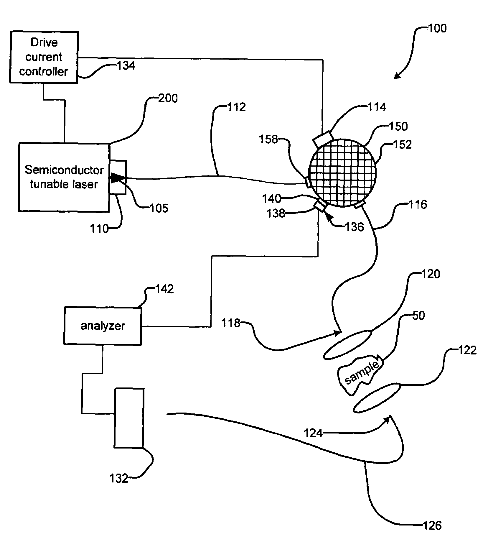
[0020]FIG. 1 illustrates a spectroscopy system 100, which has been constructed according to the principles of the present invention.

[0021]Generally, the system 100 includes a semiconductor tunable laser 200. This semiconductor tunable laser has a semiconductor gain medium, such as semiconductor optical amplifier. Often these semiconductor gain mediums emit light in only one or a few spatial modes and are fiber coupled. In the example, the generated tunable optical signal 105 is coupled into an optical fiber 112 by a coupler 110.

[0022]Because of the limited number of spatial modes of the semiconductor tunable laser 200, the optical fiber 112 is often a single mode fiber. Thus, it only supports and propagates a single spatial mode.

[0023]In one further implementation, the optical fiber 112 may further be polarization controlling fibers, such as polarization maintaining or polarization stripping (only propagates a single polarization) fiber. Specifically, such a system is illustrated in...


PUM

PropertyMeasurementUnit
optical lengthaaaaaaaaaa

Abstract

A spectroscopy system comprises a tunable semiconductor laser, such as an external cavity laser, that generates a tunable signal. A detector is provided for detecting the tunable signal after interaction with a sample. In this way, the system is able to determine the spectroscopic response of the sample by tuning the laser of the scan band and monitoring the detector's response. An integrating device, such as an integrating sphere, is interposed optically between the tunable semiconductor laser and the detector. This integrating device is used to mitigate the effects of parasitic spectral noise, such as noise that is generated by speckle or the combination of single-and multi-mode optical fibers in the transmission link between the tunable semiconductor laser and the detector.

Description

BACKGROUND OF THE INVENTION[0001]A major source of parasitic spectral distortion in spectroscopy systems arises from speckle. This effect is observable in the emission of lasers: a laser beam observed scattered from a surface, such as a piece of paper, will appear to have randomly distributed bright speckles or dots, which can change with time and wavelength. This speckle pattern is the result of phase interference patterns that form at the detector plane, such as the eye observing the laser spot, and is partly a function of the minimum spectral resolution of the system and the roughness of the scattering (reflecting) surface at which the laser emission is directed. The speckle phenomenon is caused by the simultaneous spatial and spectral coherence of the light source, where spatial coherence refers to the small spatial extent, or diameter, of the light source, and spectral coherence refers to the small spectral width of the light source. In spectroscopy systems, spectral coherence ...

Claims


Application Information

Patent Timeline
Patent Type & Authority Patents(United States)
IPC IPC(8): G01N21/00
CPCG01J3/02G01J3/0218G01J3/0251G01J3/10G01J3/26G01J3/433
Inventor ATIA, WALID A.FLANDERS, DALE C.
Owner AXSUN TECH
Why Eureka
Try Eureka