Method for manufacturing a memory device having a nanocrystal charge storage region

a memory device and charge storage technology, applied in the field of memory devices, can solve the problems of large variation in the size and spacial distribution of the nanocrystals, the device cannot retain stored data or instructions when the device is turned, and the memory device is a volatile devi

Active Publication Date: 2008-05-27
SPANSION LLC
View PDF22 Cites 11 Cited by
  • Summary
  • Abstract
  • Description
  • Claims
  • Application Information

AI Technical Summary

Problems solved by technology

A volatile memory device, on the other hand, does not retain the stored data or instructions when the device is turned off.
A drawback with this procedure is that the agglomeration process is random, thus there is a large variation in the size and spacial distribution of the nanocrystals.
In addition, the mean size of the nanocrystal is sensitive to the local temperature and metal film thickness, making it difficult to control their size distribution on large diameter semiconductor wafers.
Another drawback is that formation of the control oxide layer oxidizes the nanocrystals, which degrades their charge storage capacities.
Other drawbacks of using the agglomeration process include the cost and complexity of using metals such as gold, platinum silicide, silver, and nickel to form the thin metal layer and the inability of the control oxide to sufficiently fill the spaces between small dimension nanocrystals.

Method used


Image

  • Method for manufacturing a memory device having a nanocrystal charge storage region
  • Method for manufacturing a memory device having a nanocrystal charge storage region

Examples


Embodiment Construction

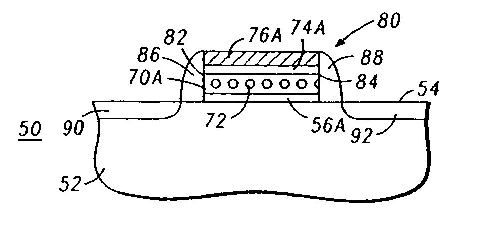
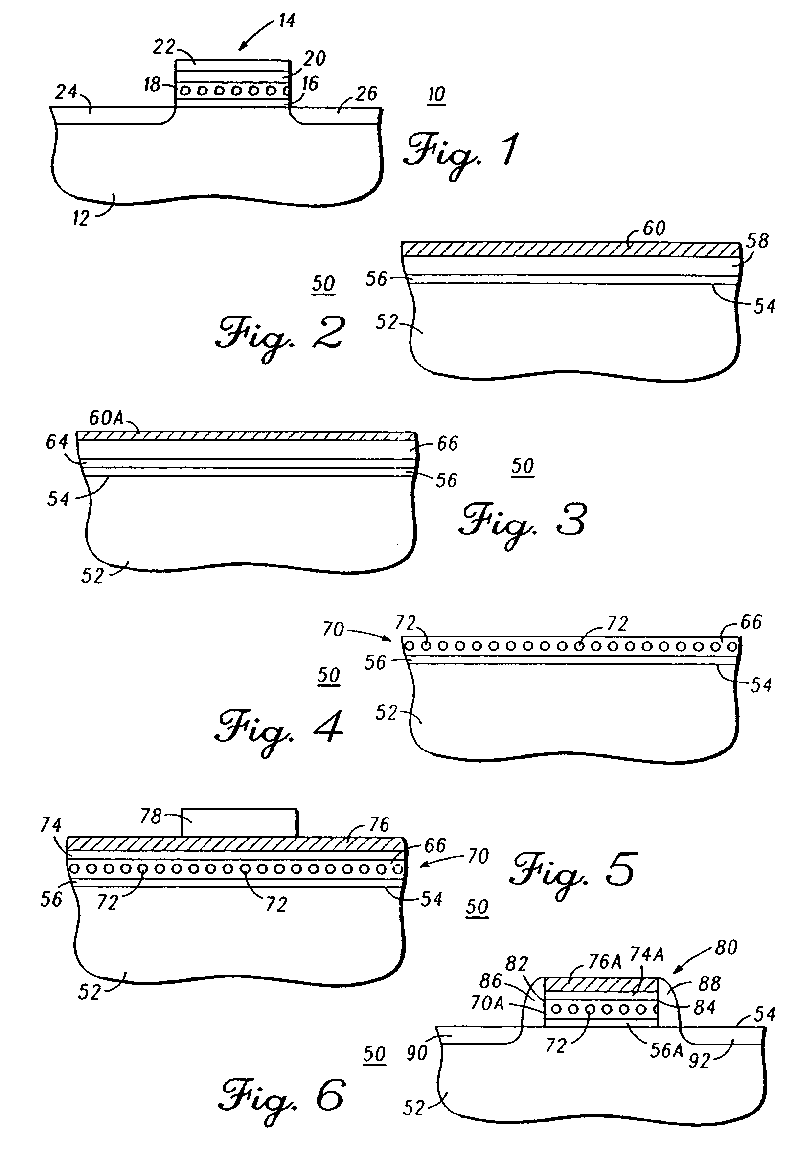
[0016]Generally, the present invention provides a method for manufacturing a memory device having a nanocrystal layer in which the nanocrystals have a uniform size and a uniform distribution. An advantage of the nanocrystal layer of the present invention is that it can be used in applications where it is desirable to have dielectric materials with high dielectric constants, i.e., dielectric constants greater than about 3.9. In accordance with an embodiment of the present invention, a metal oxide layer is formed on a tunnel oxide, and a metal layer is formed on the metal oxide layer. The metal layer is selected to have a higher heat of formation than the metal oxide layer so that under annealing conditions it reduces the metal oxide layer to metallic form which then agglomerates to form metal islands. In addition, the metal layer becomes oxidized thereby embedding the metal islands within an oxide layer to form a nanocrystal layer.

[0017]FIG. 2 is an enlarged cross-sectional side view...


PUM

PropertyMeasurementUnit
temperatureaaaaaaaaaa
dielectric constantsaaaaaaaaaa
thicknessaaaaaaaaaa

Abstract

A method for manufacturing a memory device having a metal nanocrystal charge storage structure. A substrate is provided and a first layer of dielectric material is grown on the substrate. A layer of metal oxide having a first heat of formation is formed on the first layer of dielectric material. A metal layer having a second heat of formation is formed on the metal oxide layer. The second heat of formation is greater than the first heat of formation. The metal oxide layer and the metal layer are annealed which causes the metal layer to reduce the metal oxide layer to metallic form, which then agglomerates to form metal islands. The metal layer becomes oxidized thereby embedding the metal islands within an oxide layer to form a nanocrystal layer. A control oxide is formed over the nanocrystal layer and a gate electrode is formed on the control oxide.

Description

FIELD OF THE INVENTION[0001]This invention relates, in general, to memory devices and, more particularly, to memory devices having metal nanocrystals in a charge storage region.BACKGROUND OF THE INVENTION[0002]Memory devices are used in a variety of electronic systems including computers, cellular phones, pagers, personal digital assistants, avionic systems, automotive systems, industrial control systems, appliances, etc. Depending on the particular system configuration, the memory devices may be either non-volatile or volatile. A non-volatile memory device retains the data or instructions when the device is turned off or power is removed. A volatile memory device, on the other hand, does not retain the stored data or instructions when the device is turned off. Flash memory has become an important type of non-volatile memory because it is less expensive to manufacture and has a higher device density than most other types of memory devices. In addition, Flash memory is electrically e...

Claims


Application Information

Patent Timeline
Patent Type & Authority Patents(United States)
IPC IPC(8): H01L21/8242
CPCB82Y10/00H01L21/28273H01L29/42332H01L29/7881H01L29/40114
Inventor WANG, CONNIE PIN-CHINKRIVOKAPIC, ZORANPANGRLE, SUZETTE KEEFECHIU, ROBERTYOU, LU
Owner SPANSION LLC
Why Eureka
Try Eureka