Photo-sensitive element used in electro-optical sensors to detect and convert incident light into an electrical signal

a photosensitive element and electrooptical sensor technology, applied in the field of photosensitive elements used in electrooptical sensors, can solve the problems of not being able to arbitrarily select a sub-window inside the matrix sensor, not being able to operate in an optimal manner,

Active Publication Date: 2008-05-27
ETH LAB SRL
View PDF4 Cites 0 Cited by
  • Summary
  • Abstract
  • Description
  • Claims
  • Application Information

AI Technical Summary

Benefits of technology

[0028]The presence of the external programmable reference signal is fundamental for the functioning of the photo-sensitive element, because it allows to obtain information connected to the signals that exceed the linear dynamic obtained in the traditional manner. The programmable nature of the reference signal thus guarantees the possibility of obtaining different compressions for the various lighting zones, according to the needs connected to the type of application.
[0034]In all cases, the input signal generated by the reception means advantageously has a sufficiently high value to allow an efficient processing and good immunity with respect to electric noises generated by the other components present on the support, advantageously a microchip, where the photo-sensitive element is installed.
[0036]By means of a suitable programming of the external reference it is thus possible to obtain both compressed information, exploiting only the information on the memorization element, in an identical manner to what happened in the previous implementation, and also a linear information on extended dynamics, by exploiting the combination of traditional, linear information, with that contained in the analog memory, connected to the first zeroing. Everything depends on the type of program effected by the external reference signal; in fact, it is possible to map the information in a completely linear manner using a suitable linear signal in segments.
[0038]An alternative is to surrender linearity over the whole time range, and be satisfied with a compression of the signal for higher levels of luminosity, with the advantage that it is possible to map a greater light range.
[0041]By combining this system with a suitable system to analyze the image obtained, it is also possible to achieve an adaptive system wherein the response curve of the sensor is optimized according to the distribution of intensity on the scene in question.
[0044]it provides good quality images even in conditions of low luminosity at input and hence low photo-generated current;

Problems solved by technology

The optical sensors were previously made using CCD technology (Charged-Coupled Device), which guarantees a very satisfactory image quality in the presence of well-controlled lighting, but which does not allow to operate in an optimum manner when there is a highly differentiated light inside the same scene, that is, with an input signal having high dynamics, more than 120 dB.
Furthermore, CCDs are not very versatile from various viewpoints: they cannot easily be integrated with complex driving circuits in a single silicon support, the so-called microchip, and it is not possible to arbitrarily select a sub-window inside the matrix sensor.
However, this conversion, obtained for example by connecting to the photo-sensitive element junction a MOS type transistor in diode configuration, as described in U.S. Pat. No. 5,608,204, suffers from the fundamental disadvantage of providing a low image definition in the event of low lighting.
High-resolution images are obtained by means of a linear reading of the photo-sensitive element; this technique, however, has the disadvantage that it does not give the possibility of obtaining good quality images in conditions of very diversified lighting inside the same scene.
The implementation of this known technique, using two fixed reference slopes employed in a combined manner, has the disadvantage, however, that it is necessary to realize a bulky photo-sensitive element and is therefore difficult to exploit for industrial devices, which require a high level of integration in order to achieve high-performance pixels integrated into a single silicon chip.

Method used


Image

  • Photo-sensitive element used in electro-optical sensors to detect and convert incident light into an electrical signal
  • Photo-sensitive element used in electro-optical sensors to detect and convert incident light into an electrical signal
  • Photo-sensitive element used in electro-optical sensors to detect and convert incident light into an electrical signal

Examples


Embodiment Construction

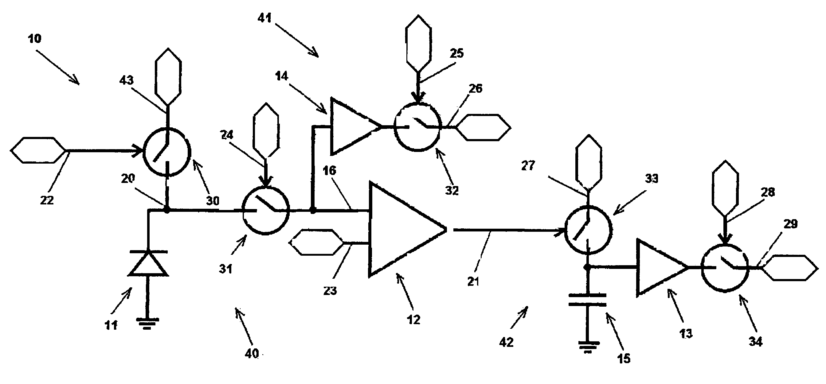
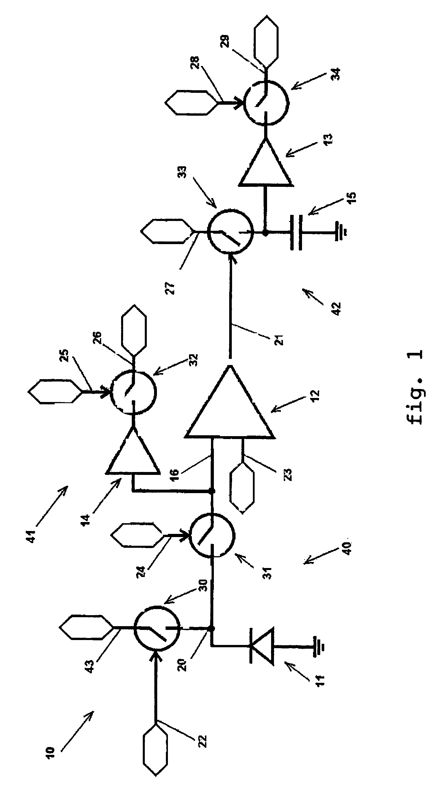
[0051]With reference to FIG. 1, a photo-sensitive element 10, or pixel, according to the present invention comprises:[0052]an element to detect and convert 40 the light signal, which comprises a photodiode 11, inversely polarized, a reset switch 30 made using semiconductor technology and driven by means of an external reset signal 22 which allows to connect an external signal 43 to a photo-sensitive node 20, and a first de-coupling switch 31 made using semiconductor technology and driven by means of a shutter control signal 24;[0053]a comparison element 12 to which two signals arrive, a threshold signal 23 and a signal 16 arriving from the photodiode 11 by means of the first de-coupling switch 31;[0054]two reading channels, respectively first 41 and second 42, of which the first 41 consists of an active amplification element 14 and a selection switch 32 made using semiconductor technology, driven by a first external selection signal 25 which leads the output signal onto a reading li...


PUM


Abstract

Photo-sensitive element for electro-optical sensors, including at least a photodiode able to generate a current that is function of the incident light, a conversion circuit able to convert the current generated into a voltage signal, a comparator able to commute if the voltage signal reaches or exceeds a determinate threshold signal, and at least a measuring and memorization element able to measure and memorize the temporal instant of commutation of the comparator and able to be driven by a reference signal in order to render available to an output line a signal estimating the incident light. The reference signal is of the type that can be programmed from outside.

Description

[0001]This application claims the priority of Italian Patent Application No. UD2005A000119 filed on 18 Jul. 2005.FIELD OF THE INVENTION[0002]The present invention concerns a photo-sensitive element used in electro-optical sensors, suitable to detect an incident light and to convert it into a correlated electric signal.[0003]The photo-sensitive element, according to the present invention, is used to achieve electro-optical sensors of the linear or two-dimensional matrix type that can be used in different devices for artificial vision, such as for example digital video cameras, intelligent optical sensors or other.[0004]The photo-sensitive element according to the invention guarantees a very satisfactory image-quality both in conditions of poor light and in the presence of uncontrolled light, hence characterized by a variable intensity in a wide range, for example to achieve electro-optical sensors used in the field of automobiles, security control, road controls and traffic controls....

Claims


Application Information

Patent Timeline
Patent Type & Authority Patents(United States)
IPC IPC(8): H01J40/14H04N5/335
CPCH04N5/335H04N25/00
Inventor STOPPA, DAVIDIT), SIMONI, ANDREAIT), VATTERONI, MONICA
Owner ETH LAB SRL
Why Eureka
Try Eureka