
Integrated passive devices

a passive device and integrated technology, applied in the direction of solid-state devices, basic electric elements, inductances, etc., can solve the problems of unrelenting pressure to produce more compact and area-efficient ipds, stacking devices on ipd substrates especially inviting problematic interactions, and inherently relatively large, so as to reduce rf interactions, reduce interactions on top of ipd substrates, and thin

Inactive Publication Date: 2008-06-03
SYCHIP
View PDF5 Cites 20 Cited by
  • Summary
  • Abstract
  • Description
  • Claims
  • Application Information

AI Technical Summary

Benefits of technology

"The patent describes a way to control electrical interactions in a way that reduces interference with sensitive components, such as RF inductor elements, in a microelectronic device. This is achieved by using a special substrate called an IPD, which helps to minimize interference and reduce the size of the device. The use of a thinner IPD substrate also reduces interactions with other components. Overall, this approach helps to create a more reliable and efficient microelectronic device."

Problems solved by technology

But, more fundamentally, the size of many passive devices is a function of the frequency of the device, and thus is inherently relatively large.
However, still, there is unrelenting pressure to produce more compact and area efficient IPDs.
However, stacking devices on an IPD substrate especially invites problematic interactions.

Method used


Image

  • Integrated passive devices
  • Integrated passive devices
  • Integrated passive devices

Examples


Embodiment Construction

[0024]The first part of the detailed description below deals with the preferred substrate for the IPD MCM.

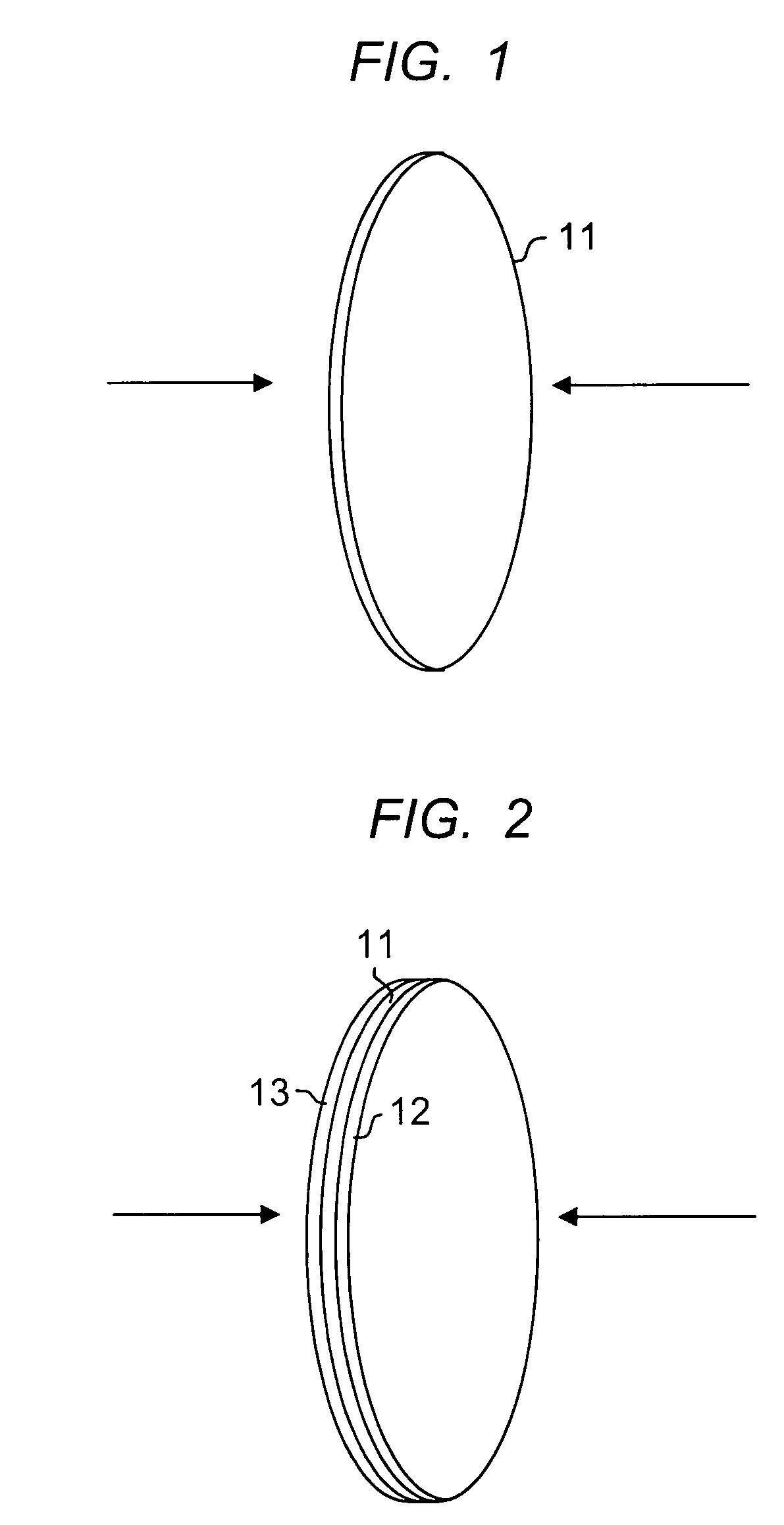
[0025]FIG. 1 is a view of a starting wafer 11. This is a single crystal silicon wafer cut from a boule, and is of a type of wafer used in enormous volume for IC device fabrication worldwide. Silicon wafers are produced in many sizes, but typically the larger the diameter of the wafer, the lower the potential device cost. Currently, silicon wafers are available in diameters up to twelve inches. With twelve inch wafers state of the art, that size will be used as the example in the following description, it being understood that smaller wafers, for example 6″ or 8″, are also useful.

[0026]In a wafer production facility, after sawing and polishing the wafers, each wafer is subjected to quality control, where the wafer is measured for conformity to rigid standards for physical size and electrical properties. Typically wafers with chips or scratches will be rejected. Wafers that have e...


PUM


Abstract

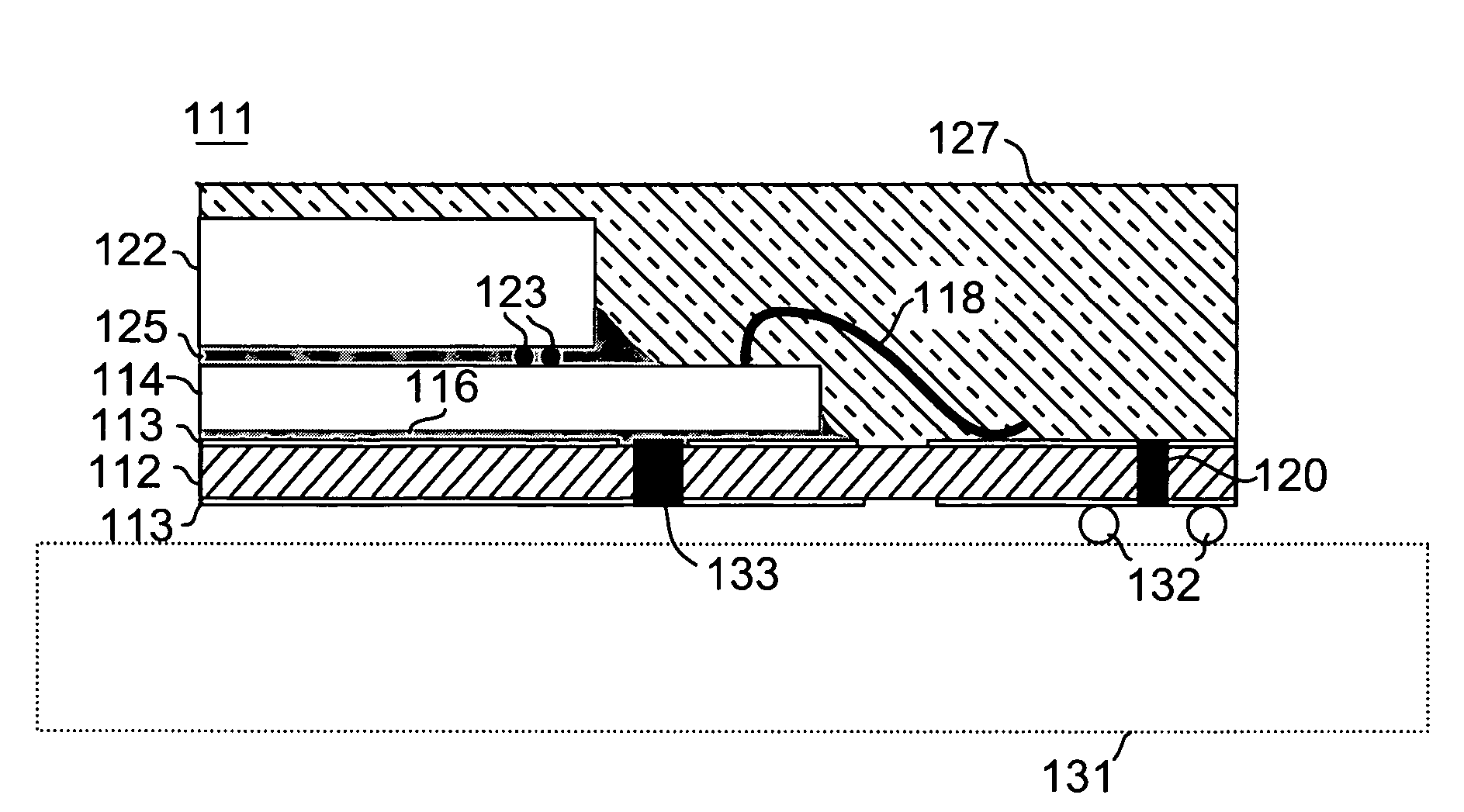
The specification describes a multi-chip module (MCM) that contains an integrated passive device (IPD) as the carrier substrate (IPD MCM). Parasitic electrical interactions are controlled at one or both interfaces of the IPD either by eliminating metal from the interfaces, or by selective use of metal in parts of the MCM that are remote from the sensitive device components. The sensitive device components are primarily analog circuit components, especially RF inductor elements. In the IPD layout, the sensitive components are segregated from other components. This allows implementation of the selective metal approach. It also allows parasitic interactions on top of the IPD substrate to be reduced by selective placement of IC semiconductor chips and IC chip ground planes. In preferred embodiments of the IPD MCM of the invention, the IPD substrate is polysilicon, to further minimize RF interactions. The various methods of assembling the module may be adapted to keep the overall thickness within 1.0 mm.

Description

[0001]This application is a continuation-in-part of application Ser. No. 10 / 835,338, filed Apr. 29, 2004 now U.S. Pat. No. 7,259,077.FIELD OF THE INVENTION[0002]This invention relates to integrated passive devices (IPDs) and more specifically to integrated circuits (IC) in the form of multi-chip modules (MCMs) where an IPD chip is a main component.BACKGROUND OF THE INVENTION[0003](Portions of the technical material contained in this section may not be prior art.)[0004]State of the art radio frequency (RF) electrical circuits use large quantities of passive devices. Many of these circuits are used in hand held wireless products. Accordingly, miniaturization of passive devices and passive device circuits is an important goal in RF device technology.[0005]Integration and miniaturization of passive devices on the scale of active silicon devices has not occurred for at least two reasons. One, typical passive devices to date employ different material technologies. But, more fundamentally,...

Claims


Application Information

Patent Timeline
Patent Type & Authority Patents(United States)
IPC IPC(8): H01L23/52H01L27/04H01L21/00H01L21/02H01L21/822H01L23/34H01L27/01H10B12/00
CPCH01L23/49833H01L23/645H01L23/66H01L25/16H01L27/016H01L28/10H01L28/20H01L28/40H01L23/49822H01L23/49816H01L2924/1461H01L24/16H01L24/48H01L2224/16145H01L2224/48091H01L2225/06513H01L2924/01078H01L2924/01079H01L2924/14H01L2924/15311H01L2924/19011H01L2924/19015H01L2924/19041H01L2924/19042H01L2924/19043H01L2924/19103H01L2924/30105H01L2924/30107H01L2924/13091H01L2924/10253H01L2224/73265H01L2224/73204H01L2224/48227H01L2224/32225H01L2224/32145H01L2224/48465H01L2924/00014H01L2924/00H01L2224/48237H01L2924/00012H01L24/73H01L2224/45099H01L2224/45015H01L2924/207H01L27/06
Inventor CHIU, ANTHONY M.DEGANI, YINONGAO, CHARLEY CHUNLEISUN, KUNQUANSUN, LIQUO
Owner SYCHIP
Learn More