Electronic device package and electronic equipment

a technology of which is applied in the direction of printed circuit manufacturing, printed circuit aspects, non-metallic protective coating applications, etc., can solve the problems of increasing the thickness of the electronic equipment and electronic components on the device, and conventional methods that are insufficient to reduce the thickness and weight of the electronic equipment and electronic components. , to achieve the effect of high resistance to bending and thinness and flexibl

Active Publication Date: 2008-06-10
SEIKO EPSON CORP
View PDF15 Cites 5 Cited by
  • Summary
  • Abstract
  • Description
  • Claims
  • Application Information

AI Technical Summary

Benefits of technology

[0011]The present invention has been realized in consideration of the above points, and an object thereof is to provide an electronic device package for mounting an electronic device to be loaded on electronic equipment and electronic components, it being possible to make the electronic device package thin and flexible so that it has high resistance to bending.

Problems solved by technology

However, in methods using anisotropic conductive materials, the anisotropic conductive material adds substantially 10 μm to 30 μm to the thickness, and accordingly increases the thickness of the electronic equipment and electronic components which the device is mounted on.
Methods using wire boding require a space of more than 1 mm for extracting the wire, and consequently increase the thickness of the electronic equipment and electronic components which the device is mounted on.
Therefore, these conventional methods are insufficient for reducing the thickness and weight of the electronic equipment and their electronic components.
In particular, when these methods are applied in the ultra-thin IC mentioned above, there is a danger that ultrasonic waves and pressure when connecting may destroy the ultra-thin IC chip and reduce the reliability of the connection.
However, the conventional mounting method described in the above Patent Application is not sufficiently resistant to bending of the electronic device package, and consequently has a problem of poor reliability when used repeatedly.
When the thickness of an IC chip is reduced to substantially 50 μm, in addition to the thickness of the chip itself, minute blemishes caused during the manufacturing process may damage the semiconductor chip.

Method used


Image

  • Electronic device package and electronic equipment
  • Electronic device package and electronic equipment
  • Electronic device package and electronic equipment

Examples


first embodiment

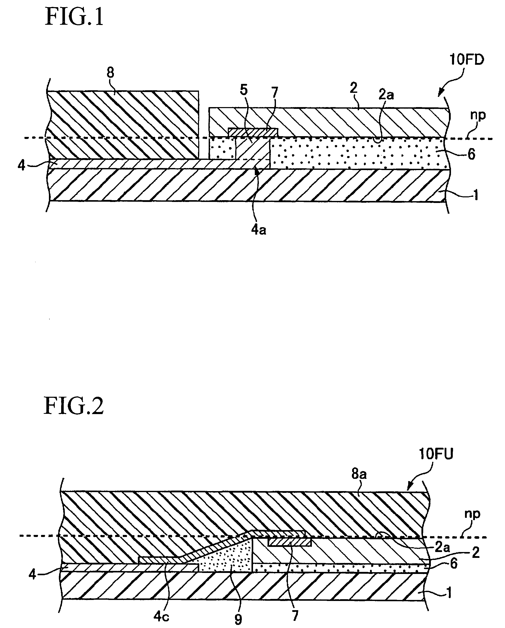
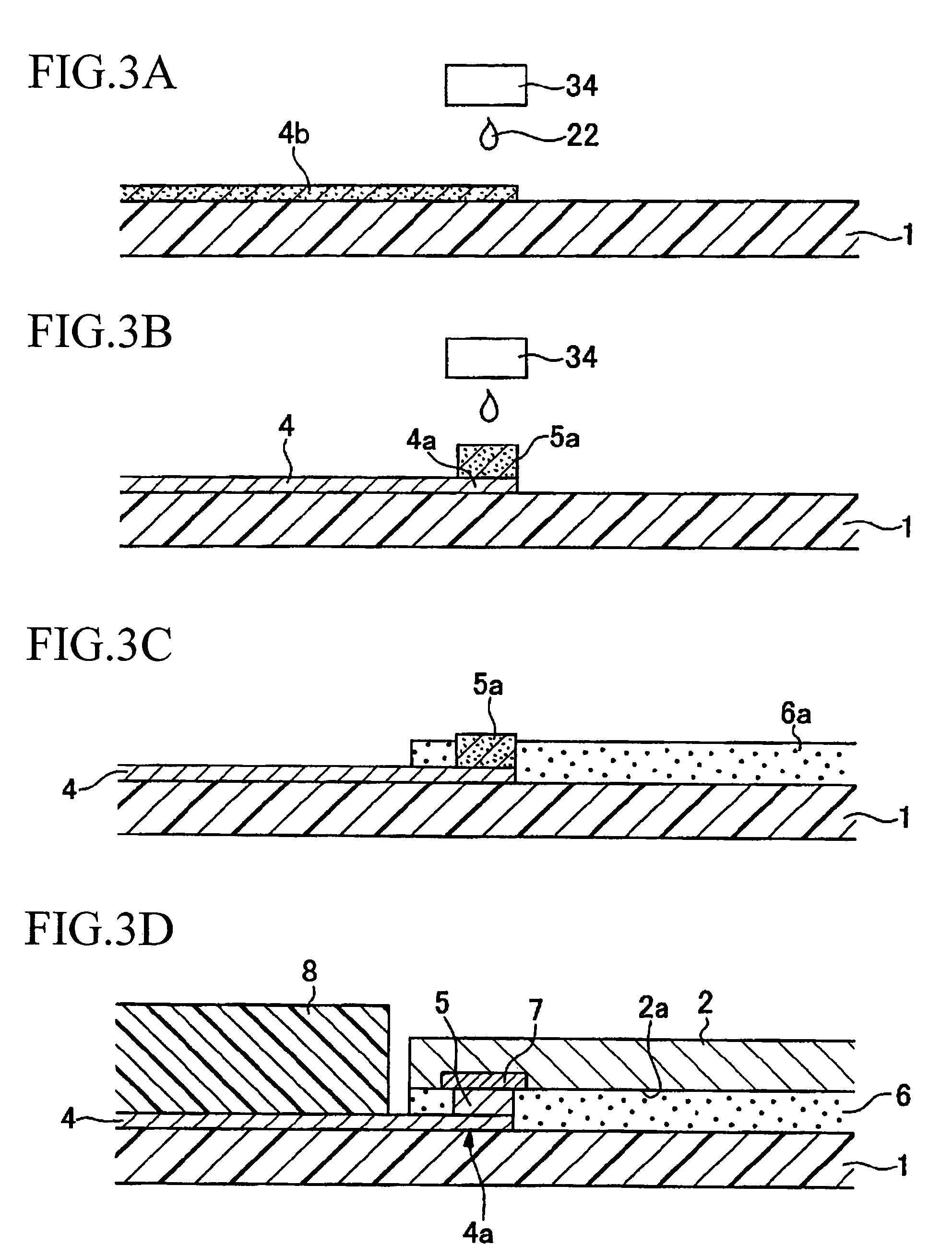
[0049]FIG. 1 is a partial cross-sectional structural view of a first embodiment of an electronic device package of this invention. As shown in FIG. 1, an electronic device package 10 FD includes a semiconductor chip (an electronic device having a connection terminal on one face) 2 which is mounted on a flexible substrate 1. Since the flexible substrate 1 consists of a resin such as polyimide, various shapes may be used such as a tape-like or a sheet-like shape.

[0050]A metal wiring pattern 4 is formed on the flexible substrate 1. Since this metal wiring pattern 4 is formed by using a metal wiring formed on the flexible substrate or a droplet ejection method that will be explained below, it is formed from a sintered compact of fine metal particles such as fine silver particles. The metal wiring pattern 4 connects to an unillustrated wiring on the end edge of the flexible substrate 1 and is connected to another external terminal (unillustrated) via this wiring. The end of the metal wir...

second embodiment

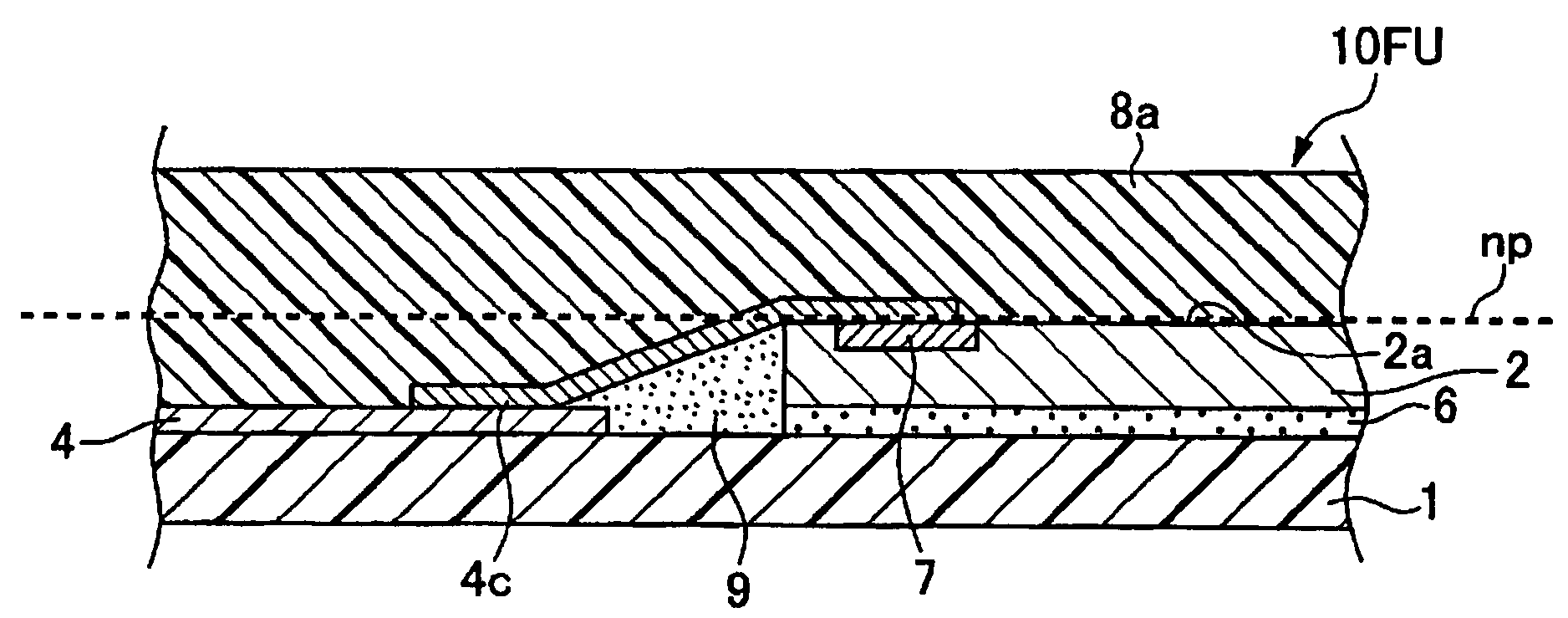
[0062]The configuration of electronic device package according to a second embodiment of this invention will be explained with reference to FIG. 2. FIG. 2 is a partial cross-sectional structural view of the electronic device package according to the second embodiment.

[0063]Other than the differences in the mount structure of the semiconductor chip 2 that constitutes the electronic device, the structure of the electronic device package 10 FU of this embodiment is the same as that of the electronic device package 10 FD in the first embodiment described above. For this reason, repetitious explanation of constituent elements in FIG. 2 which are indicated by the same reference numerals as those in FIG. 1 will be omitted.

[0064]The electronic device package 10 FU shown in FIG. 2 is produced by depositing the metal wiring pattern 4 on the metal wiring pattern 4, and then mounting the semiconductor chip 2 on top with the adhesive layer 6 in between. The semiconductor chip 2 is affixed to the...

third embodiment

[0100]Subsequently, the configuration of an electronic device package according to a third embodiment of the present invention will be explained with reference to FIG. 5. FIG. 5 is a partial cross-sectional structural view of an electronic device package according to the third embodiment.

[0101]In the third embodiment, constituent elements which are the same as those in the preceding embodiments are indicated by the same reference numerals and will not be explained further.

[0102]As shown in FIG. 5, an electronic device package 110 includes the semiconductor chip 2 mounted on the flexible substrate 1. Since the flexible substrate 1 consists of a resin such as polyimide, various shapes may be used such as a tape-like or a sheet-like shape.

[0103]The metal wiring pattern 4 is formed on the flexible substrate 1, and is connected to the pad 7 of the semiconductor chip 2 via the connection wiring 4c. The adhesive layer 6 of thermosetting insulating resin is formed on the flexible substrate ...


PUM

PropertyMeasurementUnit
thicknessaaaaaaaaaa
thicknessaaaaaaaaaa
thicknessaaaaaaaaaa

Abstract

An electronic device to be loaded on an electronic equipment or an electronic component is mounted on a mount substrate, the mount substrate being made thin and flexible and having strong resistance to bending. An electronic device package including: a flexible substrate having a wiring pattern formed thereon; and an electronic device having a terminal formation face on which a connection terminal is provided, wherein the connection terminal is electrically connected directly or via a conductive member to the wiring pattern, and the terminal formation face is substantially aligned in a neutral plane of bending in a thickness direction of the electronic device package.

Description

BACKGROUND OF THE INVENTION[0001]1. Field of the Invention[0002]This invention relates to an electronic device package and an electronic equipment.[0003]Priority is claimed on Japanese Patent Application No. 2005-204230, filed Jul. 13, 2005, Japanese Patent Application No. 2004-327710, filed Nov. 11, 2004, and Japanese Patent Application No. 2004-327711, filed Nov. 11, 2004, the contents of which are incorporated herein by reference.[0004]2. Description of Related Art[0005]Recently, starting with card-sized electronic equipment, various types of electronic equipment are becoming thinner and lighter. As electronic equipment become thinner and lighter, there is a demand for various types of electronic devices mounted thereon to be mounted in a thin state. Taking a silicon IC chip (semiconductor chip) as an example of an electronic device, it is recently becoming possible to cut away the rear face while it is in the silicon wafer state and form an ultra-thin IC chip having a thickness ...

Claims


Application Information

Patent Timeline
Patent Type & Authority Patents(United States)
IPC IPC(8): H01L23/02
CPCH01L21/563H01L23/4985H01L24/24H01L24/76H01L24/82H01L24/83H05K1/189H01L24/29H01L24/32H01L23/49883H01L2224/16225H01L2224/24011H01L2224/24051H01L2224/24226H01L2224/24998H01L2224/32225H01L2224/73203H01L2224/73204H01L2224/73267H01L2224/76155H01L2224/83192H01L2224/838H01L2224/92H01L2224/92244H01L2924/01002H01L2924/01005H01L2924/01013H01L2924/01015H01L2924/01029H01L2924/01033H01L2924/01046H01L2924/01047H01L2924/0105H01L2924/01074H01L2924/01078H01L2924/01079H01L2924/01082H01L2924/01093H01L2924/12044H01L2924/14H01L2924/19043H05K1/0393H05K1/095H05K3/1241H05K3/28H05K3/284H05K3/32H05K2201/10674H01L2224/2919H01L2924/01006H01L2924/0665H01L2224/82007H01L2224/82102H01L2224/83H01L2224/82H01L2924/00H01L2924/3512H01L24/05H01L2224/05001H01L2224/05124H01L2224/05155H01L2224/0557H01L2224/05571H01L2224/05573H01L2224/0558H01L2224/05644H01L2924/181H01L2924/00014H01L2924/00012
Inventor ITO, WATARU
Owner SEIKO EPSON CORP
Why Eureka
Try Eureka