Post fabrication CD modification on imprint lithography mask

a technology of imprint lithography and post fabrication, which is applied in the field of photolithographic systems and methods, can solve the problems of increasing the cost of mask fabrication, and achieve the effect of economic benefit and greater efficiency

Inactive Publication Date: 2008-06-10
GLOBALFOUNDRIES INC
View PDF5 Cites 17 Cited by
  • Summary
  • Abstract
  • Description
  • Claims
  • Application Information

AI Technical Summary

Benefits of technology

[0008]According to another aspect of the invention, inferences can be made regarding, for example, whether to initiate compensatory action to correct detected imprint mask critical dimension error. Such inferences can be based on, for example, information related to the severity of the critical dimension error, the percentage of error (e.g., based upon t

Problems solved by technology

Current methods of pattern line formation on a photolithography mask typically pr

Method used


Image

  • Post fabrication CD modification on imprint lithography mask
  • Post fabrication CD modification on imprint lithography mask
  • Post fabrication CD modification on imprint lithography mask

Examples


Embodiment Construction

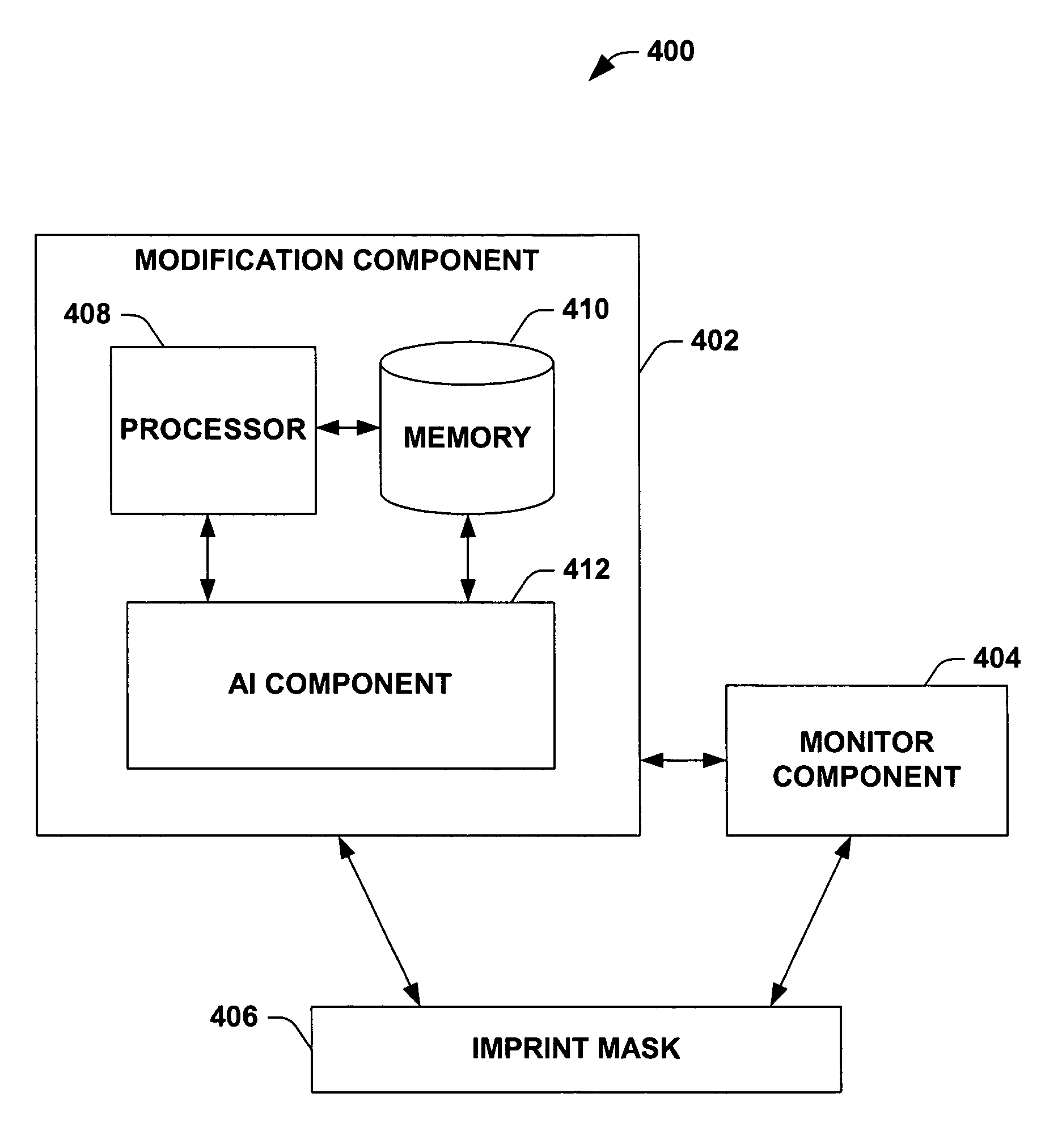
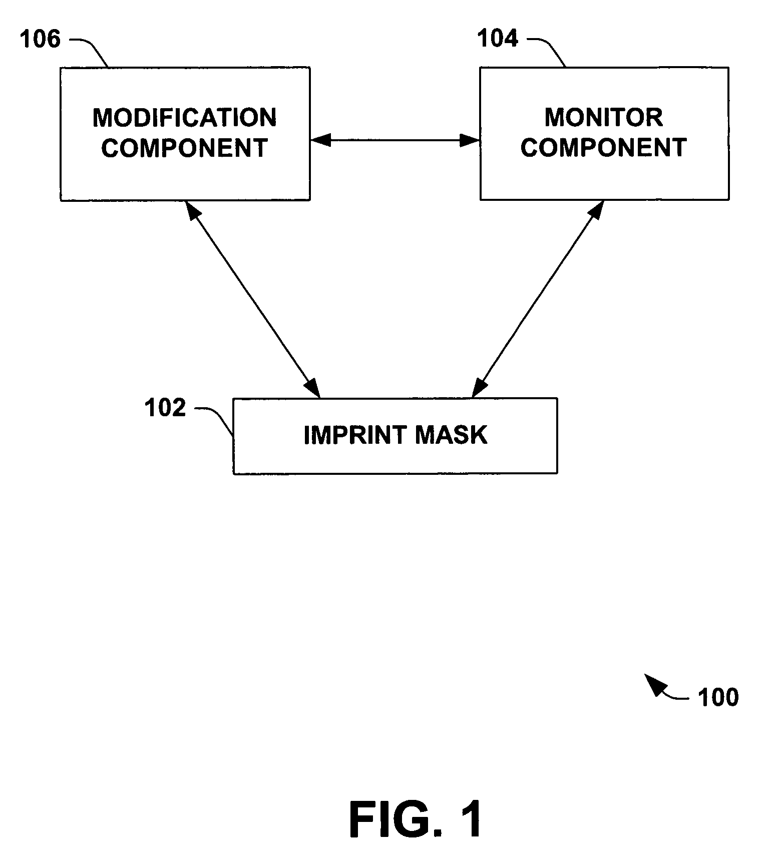
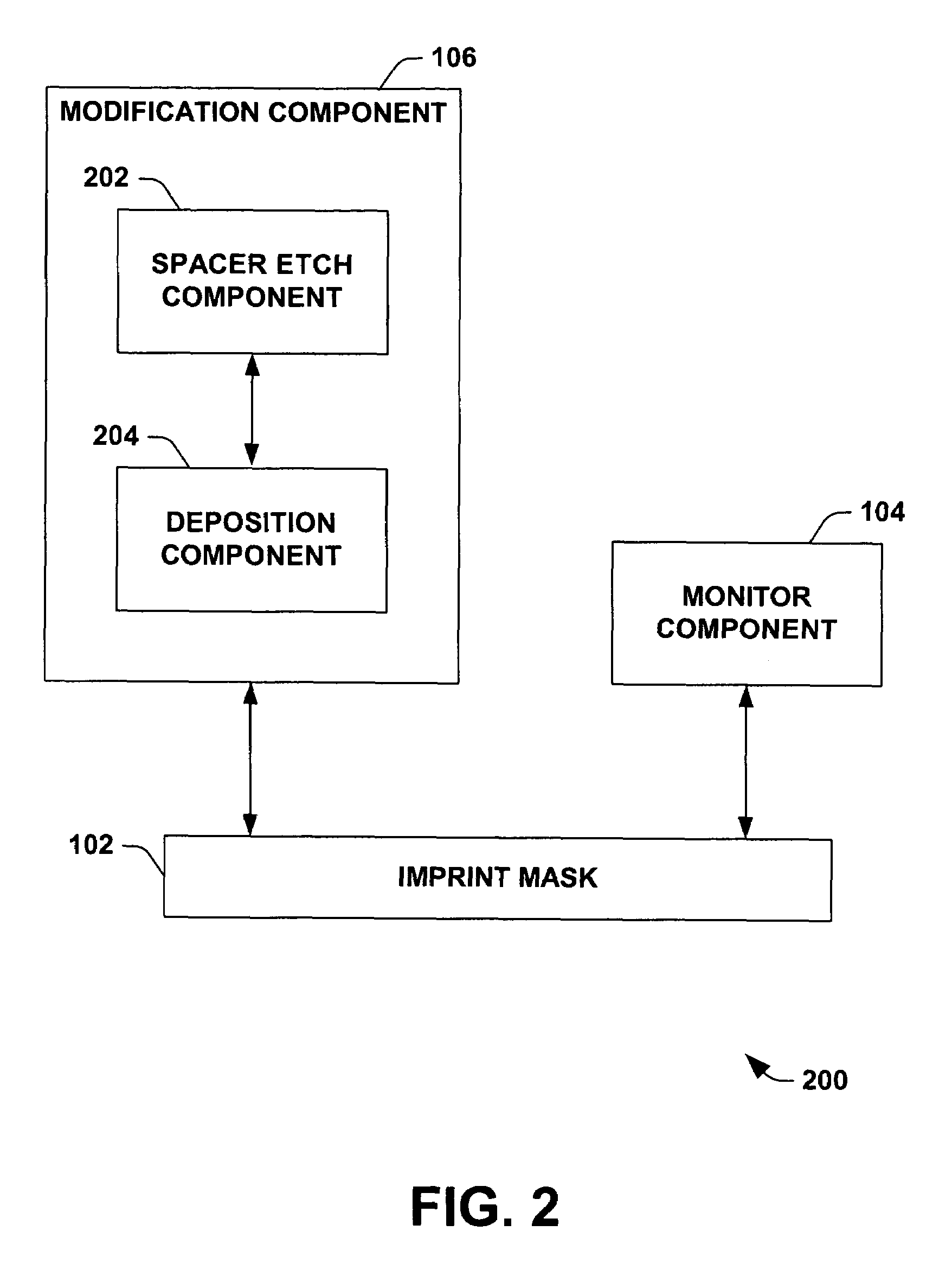
[0021]The present invention will now be described with reference to the drawings, wherein like reference numerals are used to refer to like elements throughout. The present invention will be described with reference to systems and methods for mitigating retrograde profiles on imprint mask features. It should be understood that the description of these exemplary aspects are merely illustrative and that they should not be taken in a limiting sense.

[0022]The term “component” refers to a computer-related entity, either hardware, a combination of hardware and software, software, or software in execution. For example, a component can be a process running on a processor, a processor, an object, an executable, a thread of execution, a program and a computer. By way of illustration, both an application running on a server and the server can be components. A component can reside in one physical location (e.g., in one computer) and / or can be distributed between two or more cooperating location...


PUM


Abstract

The present invention relates generally to photolithographic systems and methods, and more particularly to systems and methodologies that facilitate compensating for imprint mask critical dimension error(s). An aspect of the invention generates feedback information that facilitates control of imprint mask critical dimension via employing a scatterometry system to detect imprint mask critical dimension error, and mitigating the error via a spacer etchback procedure.

Description

TECHNICAL FIELD[0001]The present invention relates generally to photolithographic systems and methods, and more particularly to systems and methodologies that modify post imprint mask fabrication critical dimension (CD).BACKGROUND OF THE INVENTION[0002]As semiconductor trends continue toward decreased size and increased packaging density, every aspect of semiconductor fabrication processes is scrutinized in an attempt to maximize efficiency in semiconductor fabrication and throughput. Many factors contribute to fabrication of a semiconductor. For example, at least one photolithographic process can be used during fabrication of a semiconductor. This particular factor in the fabrication process is highly scrutinized by the semiconductor industry in order to improve packaging density and precision in semiconductor structure.[0003]Lithography is a process in semiconductor fabrication that generally relates to transfer of patterns between media. More specifically, lithography refers to t...

Claims


Application Information

Patent Timeline
IPC IPC(8): G06K9/00
CPCB82Y10/00B82Y40/00G03F7/0002H01L21/67242
Inventor DAKSHINA-MURTHY, SRIKANTESWARASINGH, BHANWARSUBRAMANIAN, RAMKUMAR
Owner GLOBALFOUNDRIES INC
Why Eureka
Try Eureka