Selective stress engineering for SRAM stability improvement

a selective stress engineering and stability improvement technology, applied in the field of integrated circuits, can solve the problems of severely affecting sram stability and unimproved beta ratio, and achieve the effect of significantly improving the overall stability of inventive ic and significantly improving the beta ratio between pull-down and pass-gate transistors

Inactive Publication Date: 2008-06-17
IBM CORP +1
View PDF2 Cites 16 Cited by
  • Summary
  • Abstract
  • Description
  • Claims
  • Application Information

AI Technical Summary

Benefits of technology

[0008]The present invention provides an IC including a SRAM cell wherein the beta ratio between the pull-down and pass-gate transistors is significantly improved. As a result of the improvement in the beta ratio between the transistors, the overall stability of the inventive IC is significantly improved compared to that of a conventional SRAM cell.
[0010]This desired result is achieved in the present invention by implementing a selective stress memorization technique on logic complementary metal oxide semiconductor (CMOS) nFETs and SRAM pull-down transistors to improve the performance of the aforementioned transistors. The selective stress memorization technique is not performed at the pFET region to avoid performance degradation as well as at the SRAM pass-gate transistors to avoid the improvement. With performance improvement at the pull-down transistors and no performance improvement at the pass-gate transistors, the beta ratio of the SRAM transistors is improved.

Problems solved by technology

However, SRAM stability is severely impacted by scaling.
Small mismatches in the devices during processing can cause the cell to favor one of the states, either a ‘1’ or a ‘0’.
Mismatches can result from dislocations between the drain and the source or from dopant implantation or thermal anneal temperature fluctuation.
In such prior art structures, improved device performance of both the pull-down and pass-gate transistors can be obtained, however, the beta ratio is not improved.

Method used


Image

  • Selective stress engineering for SRAM stability improvement
  • Selective stress engineering for SRAM stability improvement
  • Selective stress engineering for SRAM stability improvement

Examples


Embodiment Construction

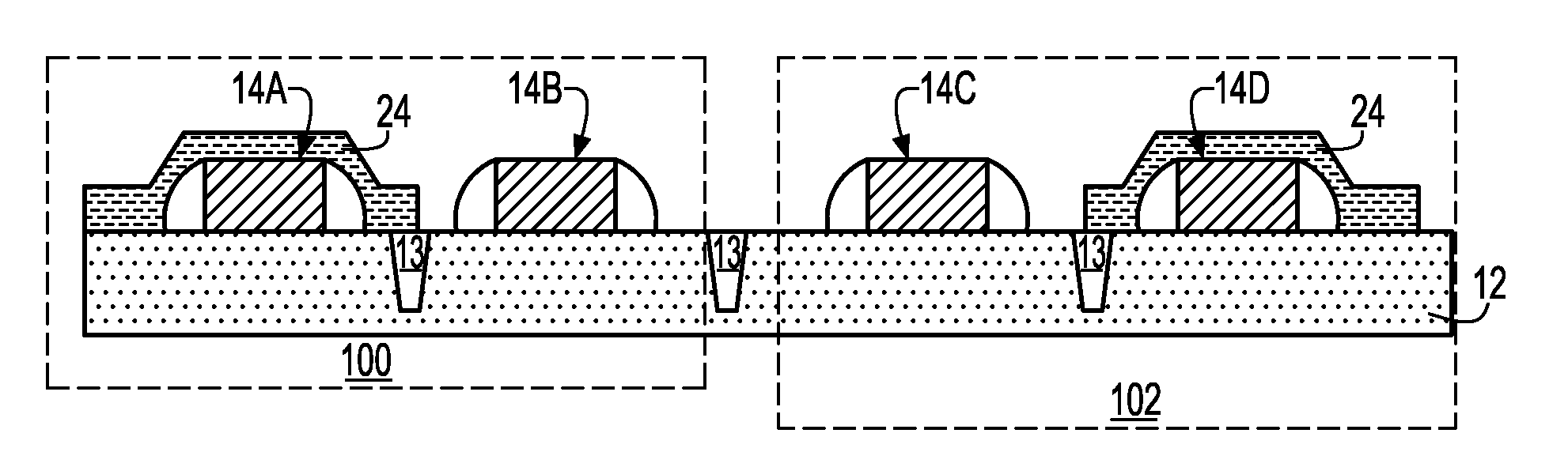
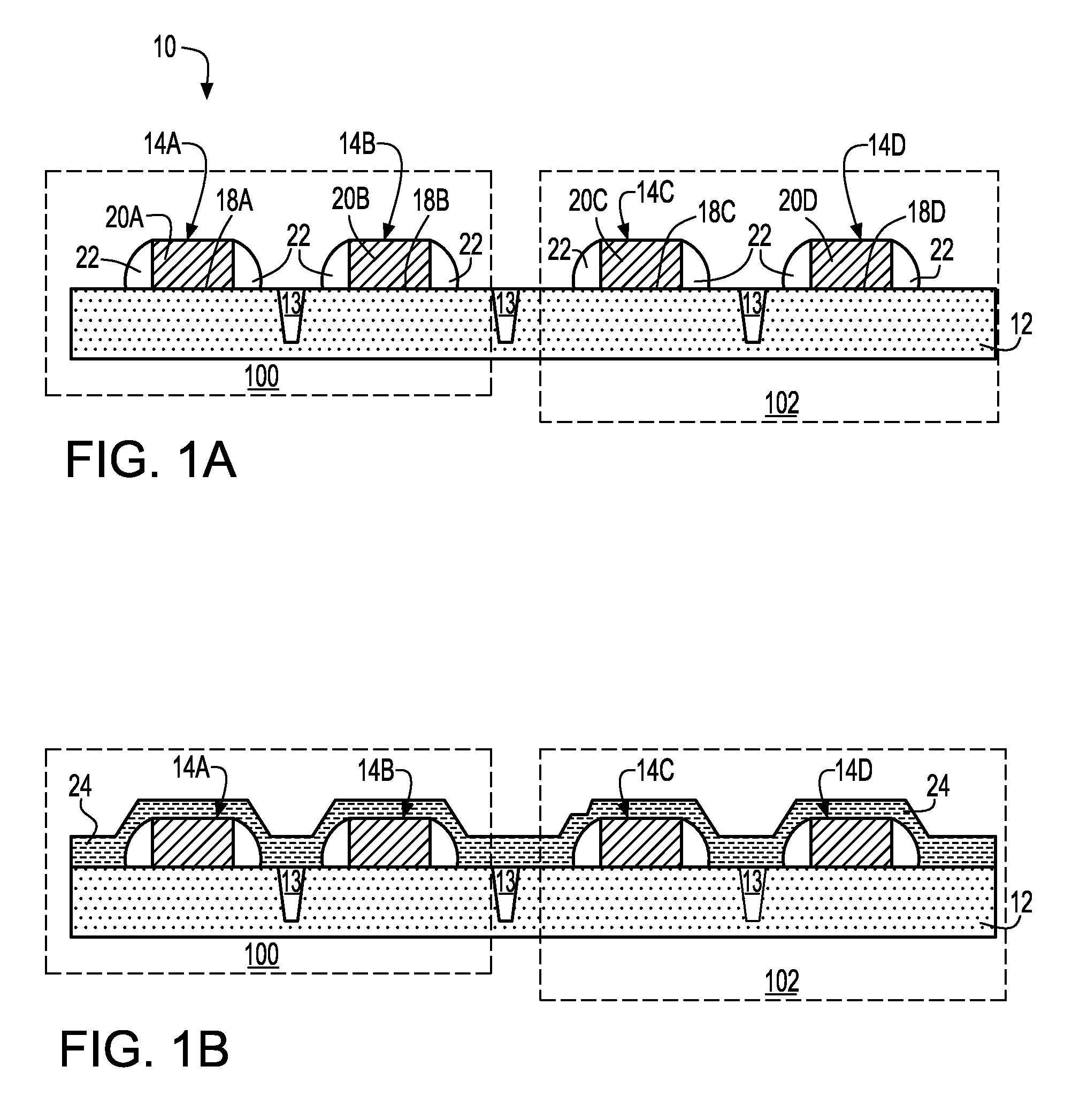
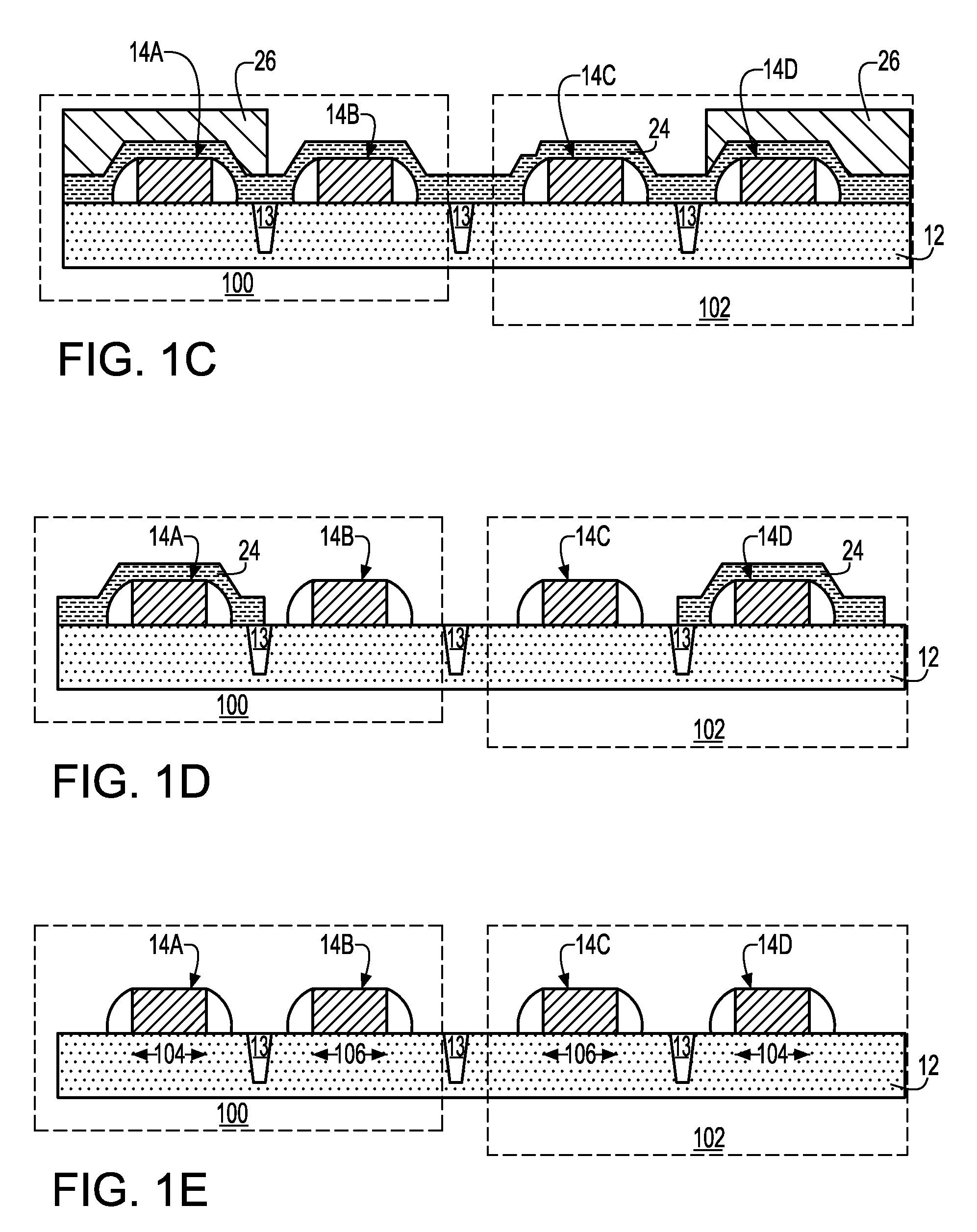
[0016]The present invention, which provides a selective stress engineering technique to increase the stability of a SRAM cell as well as the resultant IC that is fabricated utilizing the same, will now be described in greater detail by referring to the following discussion and drawings that accompany the present application. The drawings of the present application are provided for illustrative purposes and, as such, they are not drawn to scale.

[0017]In the following description, numerous specific details are set forth, such as particular structures, components, materials, dimensions, processing steps and techniques, in order to provide a thorough understanding of the present invention. However, it will be appreciated by one of ordinary skill in the art that the invention may be practiced without these specific details. In other instances, well-known structures or processing steps have not been described in detail in order to avoid obscuring the invention.

[0018]It will be understood ...


PUM


Abstract

An integrated circuit (IC) structure including a SRAM cell is provided in which the performance of the pass-gate transistors is degraded in order to increase the beta ratio of the transistors within the SRAM cell. In particular, the increased beta ratio is obtained in the present invention by intentionally improving only the performance of the pull-down transistors, while degrading the performance of the pass-gate transistors. This result is achieved in the present invention by implementing stress memorization technique on logic complementary metal oxide semiconductor (CMOS) nFETs and SRAM pull-down transistors to improve the nFET performance. The stress memorization technique is not performed at the pFET region to avoid performance degradation as well as at the SRAM pass-gate transistors to avoid the improvement. With performance improvement at the pull-down transistors and no performance improvement at the pass-gate transistors, the beta ratio of the SRAM transistors is improved.

Description

FIELD OF THE INVENTION[0001]The present invention relates to an integrated circuit (IC) and more particularly, to an IC including a static random access memory (SRAM) having improved stability.BACKGROUND OF THE INVENTION[0002]The shrinking of metal oxide semiconductor field effect transistor (MOSFET) dimensions for high density, low power and enhanced performance requires reduced power supply voltages. As a result, dielectric thickness and channel length of the transistors are scaled with power supply voltage.[0003]A static random access memory (SRAM) is a significant memory device due to its high speed, low power consumption, and simple operation. Unlike a dynamic random access memory (DRAM) cell, the SRAM does not need to regularly refresh the stored data and it has a straightforward design. However, SRAM stability is severely impacted by scaling. Small mismatches in the devices during processing can cause the cell to favor one of the states, either a ‘1’ or a ‘0’. Mismatches can ...

Claims


Application Information

Patent Timeline
Patent Type & Authority Patents(United States)
IPC IPC(8): H01L29/78
CPCH01L27/11H01L29/7847Y10S257/903H10B10/00G11C11/41
Inventor CHEN, XIANGDONGKO, YOUNG G.YANG, HAINING
Owner IBM CORP
Why Eureka
Try Eureka