One-time programable memory with additional programming time to ensure hard breakdown of the gate insulating film

a one-time programable memory and gate insulating film technology, applied in static storage, digital storage, instruments, etc., can solve the problems of increased electrical stress, reduced read current, and circuits with excessive stress

Inactive Publication Date: 2008-06-17
KK TOSHIBA
View PDF6 Cites 18 Cited by
  • Summary
  • Abstract
  • Description
  • Claims
  • Application Information

AI Technical Summary

Problems solved by technology

If, however, the current continues to flow for a longer time than required, an excessive stress is applied to circuits other than the anti-fuse element including the gate insulating film.
For example, there occurs a problem that read current is reduced by hollows caused in wires by migration due to a large amount of current.
If, however, these measures are taken, it is likely that a greater electrical stress will be applied to a number of anti-fuse elements whose gate insulating films are broken down at early time.
It is not favorable in terms of reliability.
This method has the problems that the electrical energy applied to the broken gate insulating film cannot be controlled appropriately and the device increases in size as the storage capacity becomes large.

Method used


Image

  • One-time programable memory with additional programming time to ensure hard breakdown of the gate insulating film
  • One-time programable memory with additional programming time to ensure hard breakdown of the gate insulating film
  • One-time programable memory with additional programming time to ensure hard breakdown of the gate insulating film

Examples


first embodiment

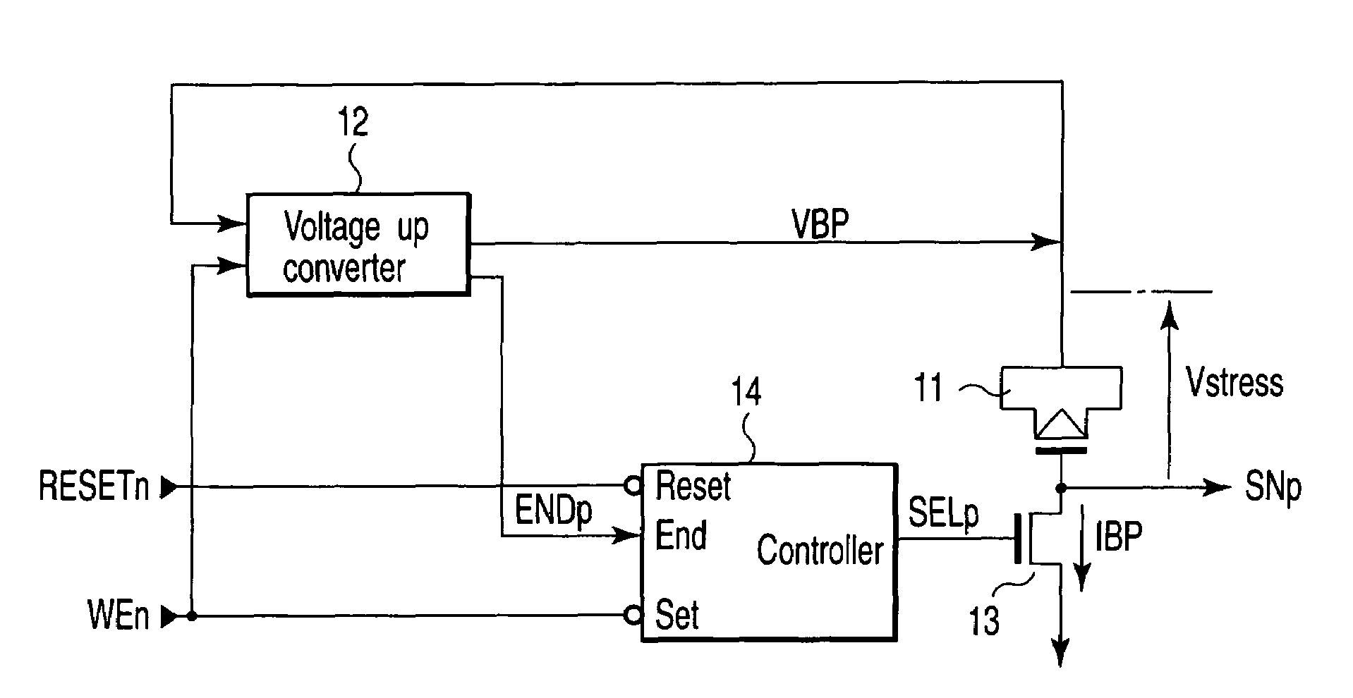
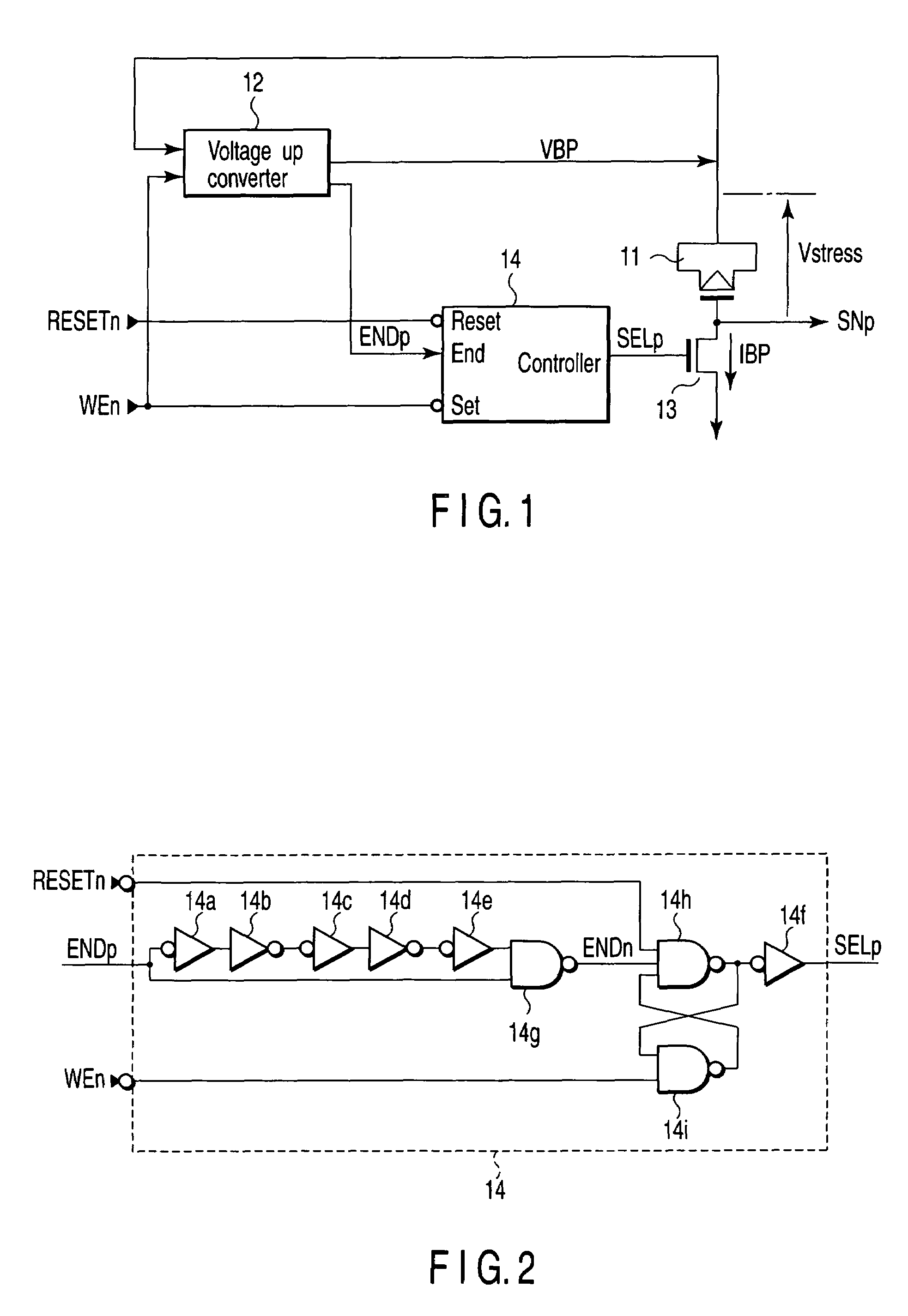
[0030]FIG. 1 shows a basic arrangement of an OTP memory (nonvolatile semiconductor memory device) according to a first embodiment of the present invention. The OTP memory uses an anti-fuse element (a semiconductor element having a MOS structure) as a storage element and can be written with information only once. In the first embodiment, the OTP memory includes an internal step-up power supply that generates a high voltage VBP (e.g., 7 V) for writing as a first voltage to be applied to the anti-fuse element based on a relatively low voltage (e.g., 2.5 V) supplied from the outside.

[0031]Referring to FIG. 1, an internal step-up power supply (voltage up converter) 12 serving as a power supply circuit is connected to one end (source / drain) of an anti-fuse element 11 corresponding to an insulating film breakdown type storage element that is programmed with information. One of the source and drain of an n-type MOS transistor serving as an open / close switch (control switch) 13 is connected ...

second embodiment

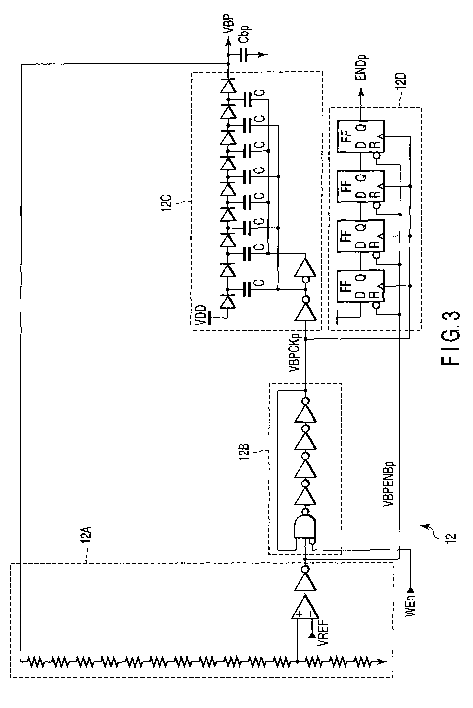
[0077]FIG. 7 shows an arrangement of an internal step-up power supply (power supply circuit) in an OTP memory (nonvolatile semiconductor memory device) according to a second embodiment of the present invention. The OTP memory uses an anti-fuse element (a semiconductor element having a MOS structure) as a storage element and can be written with information only once.

[0078]The internal step-up power supply 12′ according to the second embodiment includes a potential sensing circuit (sensing circuit) 12A′, an oscillator 12B′, a charge pump circuit (voltage generation circuit) 12C′, a replenished charge measuring device (counter circuit) 12D′ and a load capacitor Cbp. The circuits 12A′ and 12C′ make up a feedback loop to generate a high voltage VBP stably.

[0079]The potential sensing circuit 12A′ compares a step-up power supply voltage VBP with a reference power supply voltage VREF and controls the power supply current to be supplied to the charge pump circuit 12C′ to keep the step-up pow...

third embodiment

[0089]FIG. 8 shows an arrangement of an OTP memory (nonvolatile semiconductor memory device) according to a third embodiment of the present invention. The OTP memory uses an anti-fuse element (a semiconductor element having a MOS structure) as a storage element and can be written with information only once. In the third embodiment, the OTP memory includes sixty-four repetitive units (storage cells) 41 that stores 64-bit information and an internal step-up power supply 12′ as shown in FIG. 7. The same components as those of the second and third embodiment are denoted by the same reference numerals and their detailed descriptions are omitted.

[0090]Each (for one bit) of the repetitive units 41 includes an information storage unit having an anti-fuse element (insulating film breakdown type storage element) 11, a potential barrier (protection transistor) 18, an open / close switch (control switch) 13 and a sense amplifier 19. Each of the repetitive units 41 also includes a control circuit ...


PUM


Abstract

A nonvolatile semiconductor memory device includes a storage element which is programmed with information by breaking an insulating film by application of electrical stress to the storage element, a control switch which controls the application of electrical stress to the storage element, and a control circuit which controls conduction / nonconduction of the control switch. The device further includes a power supply circuit including a voltage generation circuit which generates a first voltage to cause the electrical stress in program operation, a sensing circuit which senses that the insulating film is broken down, and a counter circuit which controls the control circuit to interrupt the application of electrical stress to the storage element when a given period of time elapses after the sensing circuit senses that the insulating film is broken down.

Description

CROSS-REFERENCE TO RELATED APPLICATIONS[0001]This application is based upon and claims the benefit of priority from prior Japanese Patent Application No. 2005-006434, filed Jan. 13, 2005, the entire contents of which are incorporated herein by reference.BACKGROUND OF THE INVENTION[0002]1. Field of the Invention[0003]The present invention relates to a nonvolatile semiconductor memory device. More specifically, the invention relates to a one-time programmable (OTP) memory using irreversible storage elements to which information can be written only once.[0004]2. Description of the Related Art[0005]Recently, an OTP memory using storage elements of an insulating film breakdown type, such as an anti-fuse element (or an electrical-fuse element), has been proposed as an irreversible storage element. The OTP memory stores information by applying a high voltage that exceeds the maximum rating to a semiconductor element having a metal oxide semiconductor (MOS) structure and electrically breaki...

Claims


Application Information

Patent Timeline
Patent Type & Authority Patents(United States)
IPC IPC(8): G11C17/00
CPCG11C5/145G11C17/18G11C17/16
Inventor NAMEKAWA, TOSHIMASANAKANO, HIROAKIITO, HIROSHINAKAYAMA, ATSUSHIWADA, OSAMU
Owner KK TOSHIBA
Why Eureka
Try Eureka