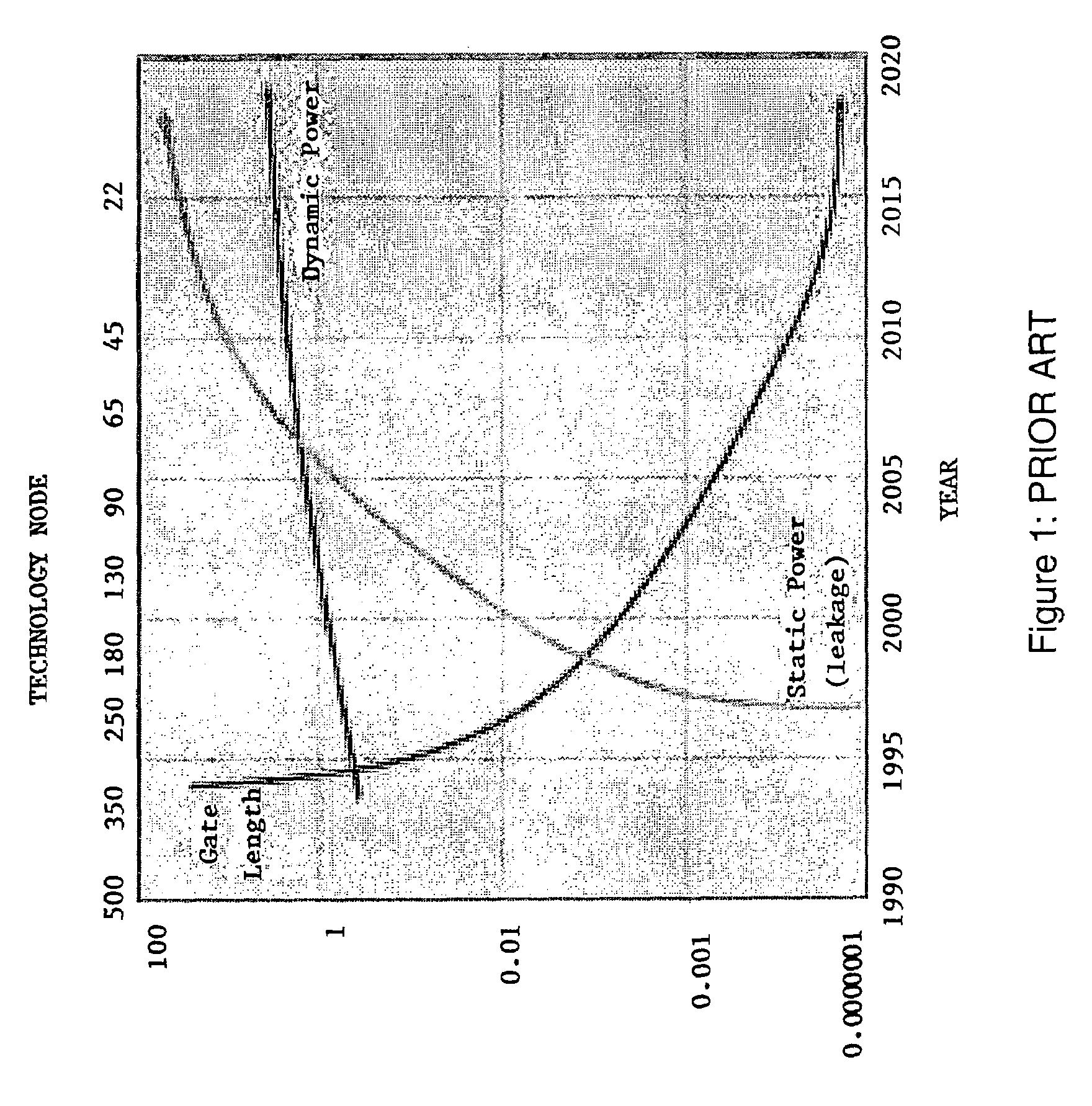
However, for sub-150 nm technologies, device
threshold voltage scaling is increasingly difficult, resulting in high FET device OFF-state leakage currents and correspondingly high static power dissipation.
Using conventional dimensional and
voltage scaling is no longer sufficient for fast dense chips, SoCs for example, so that power dissipation is setting limits on the combination of speed and function per
chip.
New generations of technology are limited by power dissipation, especially static power dissipation due to poor scaling and associated high device OFF-state leakage currents.
While this approach can reduce power dissipation for some circuits, both dynamic and static power dissipation still remains relatively high.
Both dynamic and static power are reduced in those circuits where power is turned off, however, data is not retained in registers during power OFF and will be lost unless transferred to memory at power-off and transferred back at power-on.
While this method significantly reduces both dynamic and static power, and in fact eliminates all power dissipation except for the low power shadow registers if the entire
chip is turned OFF, the shadow registers introduce significant problems of their own.
Second, static power is still dissipated in the low power shadow latches.
Also, adding a low power shadow latch for each high performance latch significantly increases
chip area which impacts chip design and reduces the number of chips per
wafer, which in turn increases chip cost.
Time-to-market with the desired product functions is vital to product success, so that typically there is insufficient time to optimize function for maximum performance at minimum total power dissipation using a more customized approach such as an optimized ASIC design, for example.
However, for sub-150 nm technologies, device
threshold voltage scaling is increasingly difficult, resulting in high FET device OFF-state leakage currents and correspondingly high static power dissipation.
New generations of technology are limited by power dissipation, especially static power dissipation due to poor scaling and resulting high device OFF-state leakage currents.
Using conventional dimensional and
voltage scaling is no longer sufficient for fast dense chips, SoCs for example, so that power dissipation is setting limits on the combination of speed and function per chip.
However, even in non-portable applications such as workstations and servers, power dissipation limitations caused by poor
CMOS technology scaling is limiting operating speeds and requiring
power management architectures.
If present single processor chip architectures and design methodologies were left unchanged, then power dissipation and latency associated with on-chip
interconnection of logic and
memory functions would become a
dominant factor resulting in power-limited chip performance.
With these new evolving chip architectures and design methodologies, limitations to chip performance are primarily due to embedded logic and
memory functions as has always been the case.
However, these embedded circuits are increasingly difficult to scale as described further above, and static power dissipation is beginning to set performance on chip operation.
It is due to leakage current that flows because of poorly scaled device threshold voltages and operating voltages.
That is, stored data is lost if power is lost or removed.
If power is removed or lost, the
logic state or data are lost.
However, volatile low power shadow latches must remain ON and therefore still dissipate power while storing logic states or data in
backup mode because the storage is volatile, and information is lost if power is lost.
Furthermore, volatile low power dissipating shadow latches use low bias current to minimize static power and are therefore very susceptible to disturb, in which stored logic states or data may be lost or corrupted.
Also, shadow latches require additional chip area that can substantially increase
chip size.
Volatile means that logic state or
data information is lost is power is lost or removed.

