Post exposure resist bake

a post-exposure resist and bake technology, applied in the field of photolithography, can solve the problems of water in the post-exposure resist, severe interference with the catalytic performance, and other defects in the completed integrated circuit, and achieve the effects of reducing the cost of production, and improving the quality of production

Inactive Publication Date: 2008-07-08
POLARIS INNOVATIONS LTD
View PDF14 Cites 38 Cited by
  • Summary
  • Abstract
  • Description
  • Claims
  • Application Information

AI Technical Summary

Benefits of technology

[0010]Still other embodiments of the invention provide a method of patterning a resist. The method comprises forming a resist on a substrate, irradiating the resist to generate a photoacid in the resist, and reacting the resist with photoacid. Preferred embodiments further include baking the resist at a temperature, sufficient to remove water from the resist before reacting the resist. Embodiments advantageously reduce the incidence of water-induced pattern defects.

Problems solved by technology

One problem encountered with chemically amplified resists is the presence of water in the post exposure resist.
The high affinity of the photo-generated proton for water severely interferes with its catalytic performance.
Spatial variations in water concentration therefore causes uneven development, which in turn causes line broadening, blobs, and other defects in the completed integrated circuit.

Method used


Image

  • Post exposure resist bake
  • Post exposure resist bake
  • Post exposure resist bake

Examples


Embodiment Construction

[0019]The making and using of preferred embodiments are discussed in detail below. It should be appreciated, however, that the present invention provides many applicable inventive concepts that may be embodied in a wide variety of specific contexts.

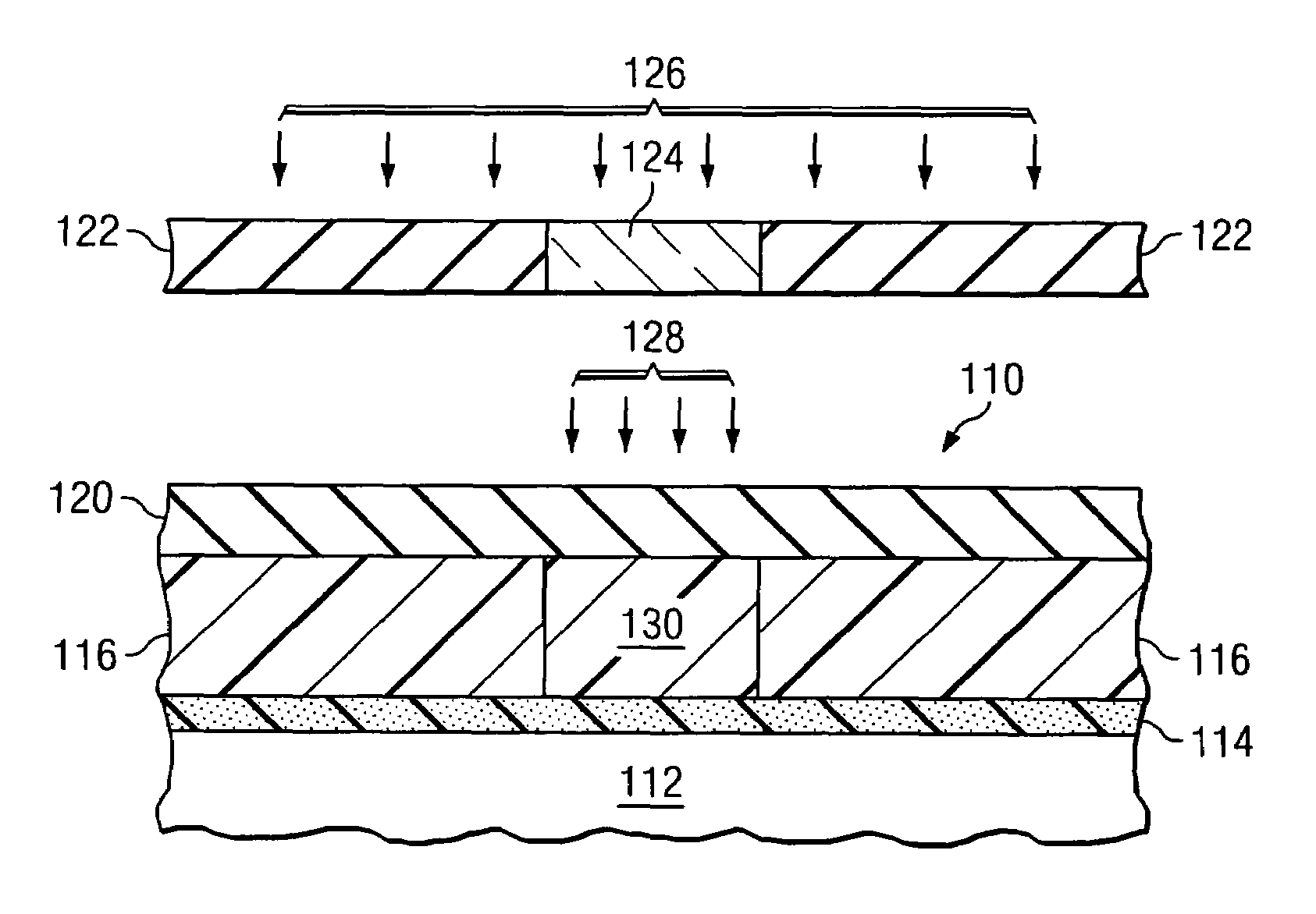
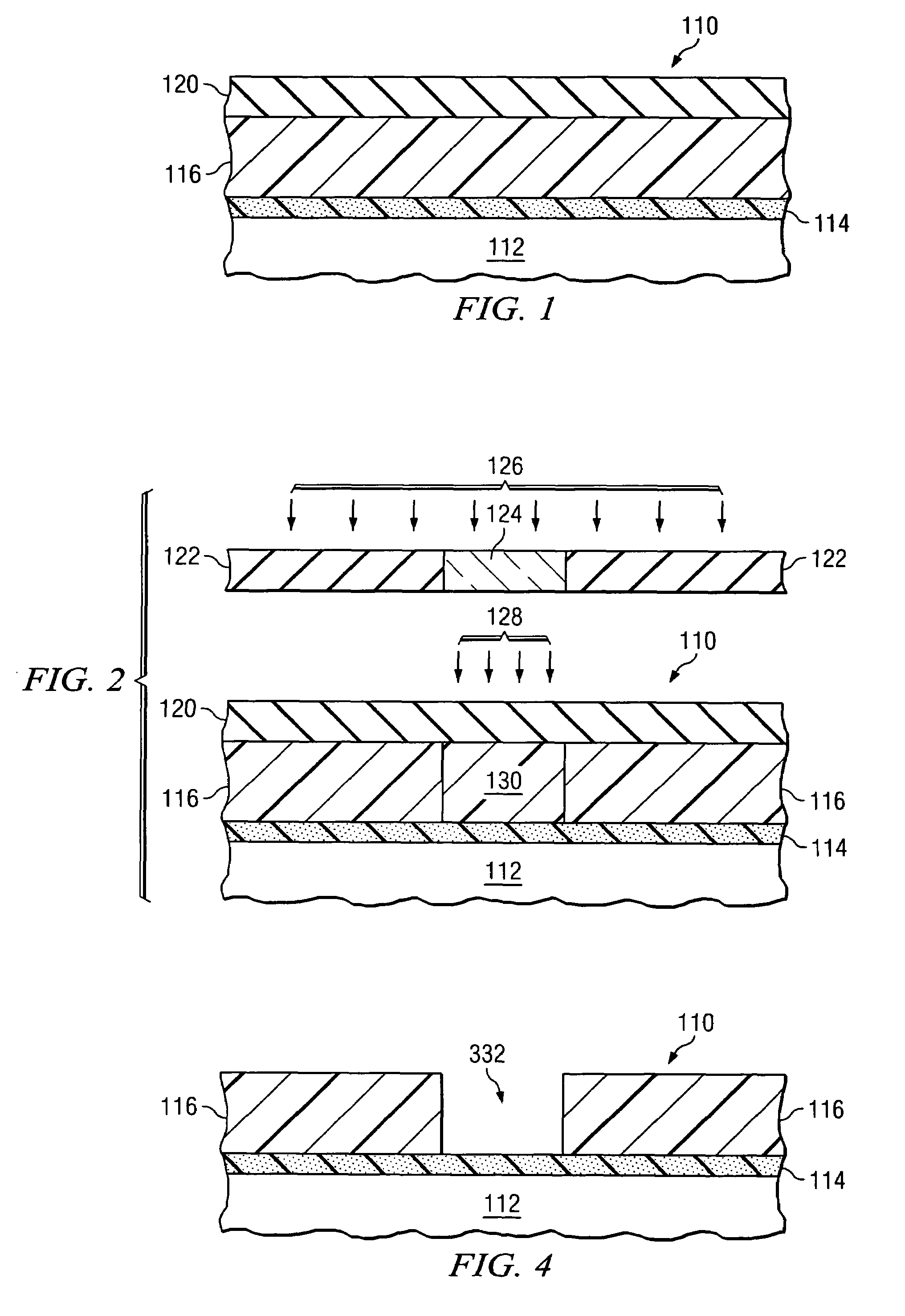
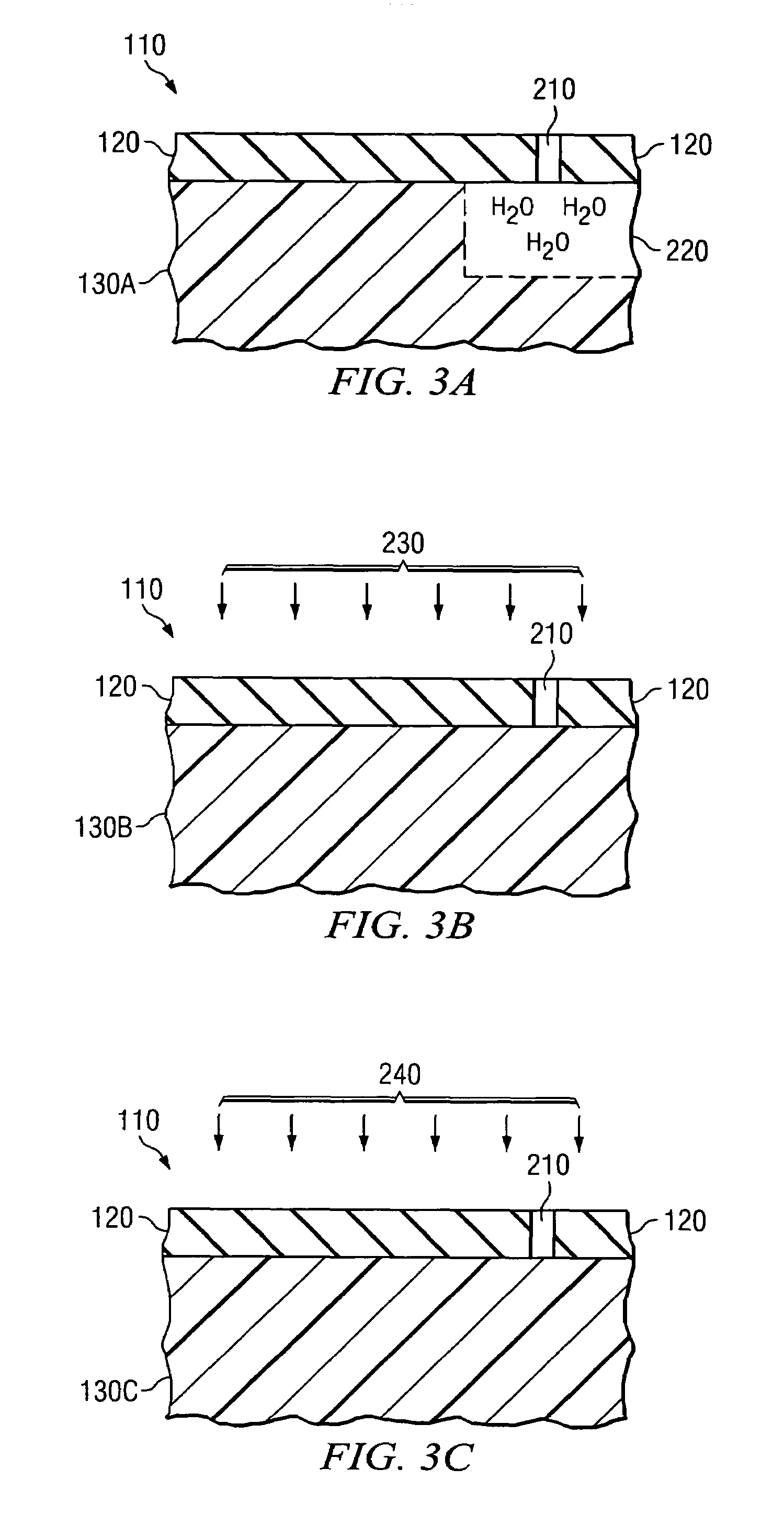
[0020]Referring now to FIG. 1, there is shown a cross sectional view of a semiconductor structure 110 comprising a semiconductor body 112 upon which has been deposited an anti-reflection coating (ARC) 114, and upon this ARC 114 has been deposited a photoresist layer 116. It is desired to expose selected areas of the photoresist layer 116 to a pattern of light that will result in these selected areas of the photoresist layer 116 being removed from the semiconductor structure 110 when the photoresist layer 116 is developed. Embodiments may further include a protective topcoat layer 120 over the photoresist layer 116. In a more particular application, preferred embodiments may be used to form a recessed feature, such as a via or a contact ho...


PUM

PropertyMeasurementUnit
temperatureaaaaaaaaaa
wavelengthaaaaaaaaaa

Abstract

A preferred embodiment of the invention provides a method for forming an integrated circuit. The method comprises forming a resist layer on a substrate. Preferably, the photoresist layer comprises a photo acid generator (PAG). Embodiments include irradiating the resist through a mask to generate a photoacid in the resist, heating the resist at a first temperature, and then heating the resist at a second temperature. Heating at the first temperature evaporates water from the resist. Heating at the second temperature deprotects the resist.

Description

TECHNICAL FIELD[0001]This invention relates generally to photolithography in the field of integrated circuit manufacture, and more particularly to a method of improving defectivity of chemically amplified resists.BACKGROUND[0002]Lithography is widely used in the manufacture of integrated circuits. In lithography, and more particularly photolithography, a photoresist layer is formed on a semiconductor substrate. The photoresist is then exposed in certain areas to actinic radiation. The areas that are irradiated are defined by a mask which is projected onto the photoresist by a lens system. The mask contains a pattern of transparent and opaque areas. The mask is exposed to actinic radiation, such as ultraviolet light (UV), which is transmitted through the transparent areas of the mask to cause a chemical reaction in corresponding regions of the photoresist.[0003]In a negative type photoresist the radiation impacted areas of the photoresist become insoluble in a developing solvent. For...

Claims


Application Information

Patent Timeline
Patent Type & Authority Patents(United States)
IPC IPC(8): B44C1/22G03F7/40
CPCH01L21/312H01L21/0273G03F7/38G03F7/0045H01L21/02118
Inventor BRANDL, STEFAN
Owner POLARIS INNOVATIONS LTD
Why Eureka
Try Eureka