Electronic device and manufacturing method of the same

a manufacturing method and technology of an electronic device, applied in the field of electronic devices, can solve the problems of requiring relatively high cost, difficulty in assembling, and difficulty in assembling, and achieve the effect of improving the reliability of the module in which a semiconductor chip and a chip component are mounted over pcb

Inactive Publication Date: 2008-07-08
RENESAS ELECTRONICS CORP
View PDF3 Cites 24 Cited by
  • Summary
  • Abstract
  • Description
  • Claims
  • Application Information

AI Technical Summary

Benefits of technology

[0009]Modules for cellular phone examined by the present inventors use ceramic substrates resistant to heat and excellent in electric insulation for module substrates over which semiconductor chips and chip components are mounted. However, the ceramic substrate has problems. It requires relatively high cost, and is easily broken by drop impact or the like. Modules for cellular phone are always required to be reduced in size and thickness; however, ceramics are easily broken when thinned. Therefore, it is difficult to reduce the thickness of an entire package in which a semiconductor chip and a chip component are mounted over a ceramic substrate and they are sealed with resin to 1 mm or below.
[0012]A semiconductor chip and a chip component are mounted over PCB, and covered and protected with insulating resin. Thereafter, the obtained module is mounted over a mother board by solder connection, and is incorporated into a product. However, during reflow processing (at 250° C. or so, for example) subsequent to the solder connection, Pb-free solder that connects the chip component to the PCB can partially melt in the module, which can lead to troubles, such as short-circuiting. Specifically, for example, semi-molten Pb-free solder flows like a flash, and connecting terminals of the chip component are joined together. This leads to short-circuiting. Where unfilled voids are formed in the narrow gap between the chip component and the PCB, this short-circuiting becomes more pronounced.
[0013]An object of the present invention is to provide a technique with which the reliability of a module using PCB for its module substrate can be enhanced.
[0019]A semiconductor chip high in adhesive strength can be mounted over PCB without damaging the PCB, and connecting terminals of a chip component can be prevented from being short-circuited to each other due to solder. Thus, the reliability of a module in which a semiconductor chip and a chip component are mounted over PCB can be enhanced.

Problems solved by technology

However, manufacturing methods of modules have various technical problems described below.
However, the ceramic substrate has problems.
It requires relatively high cost, and is easily broken by drop impact or the like.
Modules for cellular phone are always required to be reduced in size and thickness; however, ceramics are easily broken when thinned.
Therefore, it is difficult to reduce the thickness of an entire package in which a semiconductor chip and a chip component are mounted over a ceramic substrate and they are sealed with resin to 1 mm or below.
However, the present inventors found the following problems also with respect to modules using PCB for their module substrates.
Meanwhile, it poses a problem of degradation in adhesive strength.
However, this poses new problems due to high-temperature processing at 280° C. or higher.
Such problems include burning of solder resist that covers wiring formed over the surface of PCB; stripping of prepreg, which is an insulating resin sheet that constitutes PCB, from core material.

Method used


Image

  • Electronic device and manufacturing method of the same
  • Electronic device and manufacturing method of the same
  • Electronic device and manufacturing method of the same

Examples


first embodiment

[0049]In the description of the first embodiment, a case where the present invention is applied to a digital cellular phone that transmits information utilizing a GSM-based network will be taken as an example.

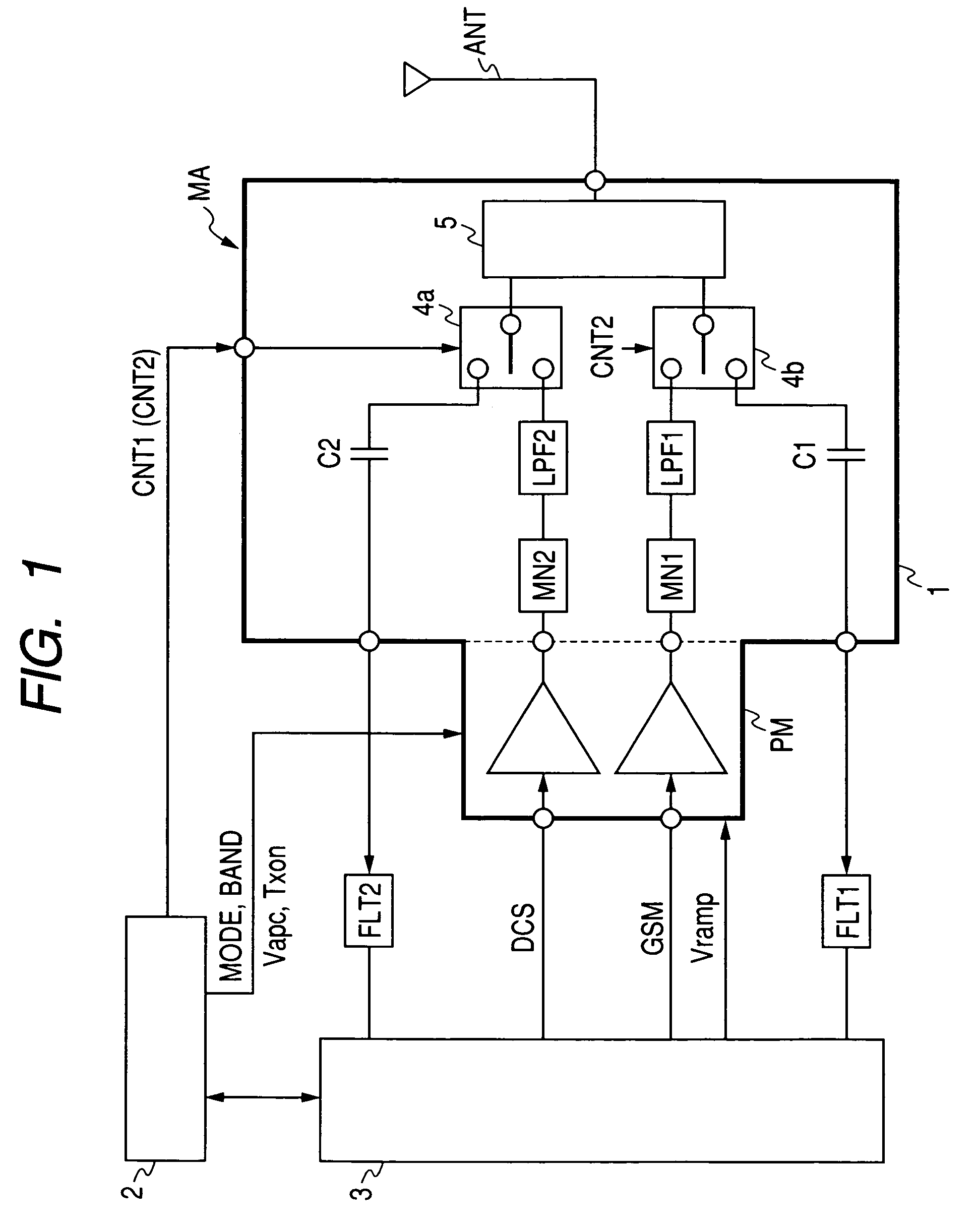
[0050]FIG. 1 illustrates an example of the system of a digital cellular phone in the first embodiment. In the figure, reference code PM denotes a power amplifier; ANT denotes an antenna for transmitting and receiving signal waves; numeral 1 denotes a front-end device; 2 denotes a baseband circuit that converts an aural signal into a baseband signal and a received signal into an aural signal, and generates a modulation method switching signal or a band switching signal; 3 denotes a circuit for modulation / demodulation that down-converts and demodulates a received signal to generate a baseband signal and modulates a transmitted signal; codes FLT1 and FLT2 denote filters that remove noise and interfering waves from a received signal. The filter FLT1 is for GSM, and the filter FLT2 ...

third embodiment

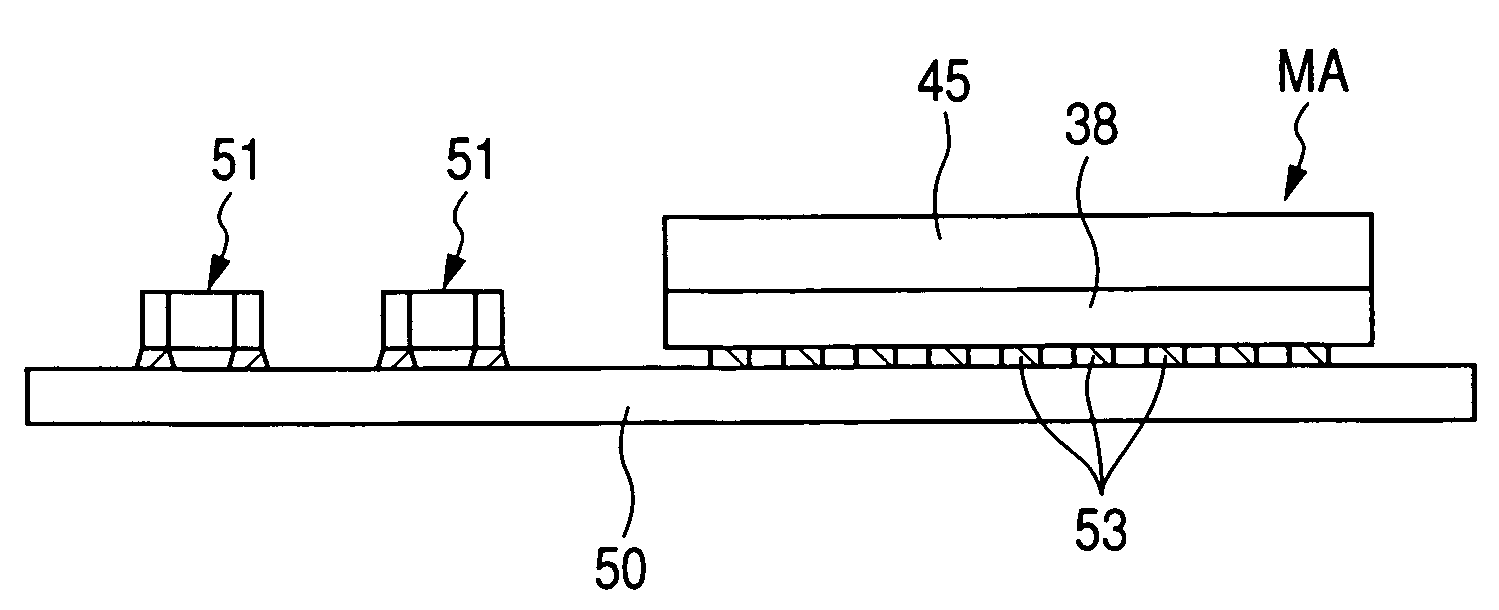
[0121]Description will be given to another example of a mounting process in which surface mount components are solder connected to a module substrate in a lump, in a third embodiment. FIG. 21 is a substantial part sectional view of a semiconductor device, explaining a mounting method following FIG. 16 associated with the first embodiment.

[0122]As in the second embodiment, a heat block 67 is not heated, and all the surface mount components mounted over PCB 38 are covered with a cover 68a. A semiconductor chip IC1 is locally heated at a temperature of 280° C. or higher, for example, a temperature of 330 to 350° C. using a hot jet 68. The semiconductor chip IC1 and substrate-side terminals 40a1 are connected with each other by high-melting point solder. Ob-free solder is melted by after heat produced when dry air jetted out of the nozzle of the hot jet 68 diffuses inside the cover 68a. A single-chip component 43 and substrate-side terminals 40b, an integrated chip component 44 and subs...

fourth embodiment

[0125]Description will be given to another example of a mounting process in which surface mount components are solder connected to a module substrate in a lump, in a fourth embodiment. FIG. 22 is a substantial part sectional view of a semiconductor device, explaining a mounting method following FIG. 16 associated with the first embodiment.

[0126]As in the second embodiment, a heat block 67 is not heated, and all the surface mount components mounted over PCB 38 are covered with a cover 68a. A semiconductor chip IC1 is locally heated at a temperature of 280° C. or higher, for example, a temperature of 330 to 350° C. using a hot jet 68. The semiconductor chip IC1 and substrate-side terminals 40a1 are connected with each other by high-melting point solder. Pb-free solder is melted by after heat produced when dry air jetted out of the nozzle of the hot jet 68 diffuses inside the cover 68a. A single-chip component 43 and substrate-side terminals 40b, an integrated chip component 44 and sub...


PUM

PropertyMeasurementUnit
thicknessaaaaaaaaaa
melting pointaaaaaaaaaa
temperatureaaaaaaaaaa

Abstract

A technique that makes it possible to enhance the reliability of a module using PCB as its module substrate is provided. Solder connection of a single-chip component 43, an integrated chip component 44, and a semiconductor chip IC2 by Pb-free solder is carried out by heat treatment at a temperature below 280° C. using a heat block. Solder connection of a semiconductor chip IC1 by high-melting point solder is carried out by heat treatment at a temperature of 280° C. or higher using a hot jet. Thus, the semiconductor chip IC1 can be solder connected to PCB 38 using high-melting point solder without the following troubles: damage to the PCB 38 due to heat, for example, burning of solder resist; and peeling of prepreg from a core material. Therefore, the semiconductor chip IC1 can be mounted over the PCB 38 with high connection strength.

Description

CROSS-REFERENCE TO RELATED APPLICATION[0001]The present application claims priority from Japanese patent application No. 2004-336113 filed on Nov. 19, 2004, the content of which is hereby incorporated by reference into this application.BACKGROUND OF THE INVENTION[0002]The present invention relates to an electronic device and a manufacturing technique thereof and in particular to a technique effectively applicable to a manufacturing method of a module.[0003]Mobile communication equipment such as cellular phone adopts a module of such a structure that the following is implemented: for example, a surface mount semiconductor chip over which a power amplifier, an antenna switch, or the like is formed and a surface mount chip component over which a capacitor, a resistor, or the like is formed are mounted over one and the same substrate. The semiconductor chip and the chip component are mounted over the module substrate by solder connection. In addition, they are covered and protected with...

Claims


Application Information

Patent Timeline
Patent Type & Authority Patents(United States)
IPC IPC(8): H01L21/44H01L21/48
CPCH01L23/3121H01L24/45H01L24/48H01L25/162H01L25/50H01L27/0617H01L27/0629H05K3/3463H05K3/3494H01L24/75H01L24/83H01L24/27H01L24/743Y10T29/49144Y10T29/49146H01L2924/1305H01L23/4824H01L23/5227H01L2224/0401H01L2224/05155H01L2224/05624H01L2224/05644H01L2224/13144H01L2224/16H01L2224/45144H01L2224/48091H01L2224/48227H01L2224/83192H01L2924/01004H01L2924/01013H01L2924/01014H01L2924/0102H01L2924/01028H01L2924/01029H01L2924/01047H01L2924/0105H01L2924/01061H01L2924/01078H01L2924/01079H01L2924/01082H01L2924/014H01L2924/10253H01L2924/10329H01L2924/13091H01L2924/19041H01L2924/19105H01L2924/3011H01L2924/3025H05K1/141H05K3/284H05K2201/045H05K2203/081H05K2203/1476H01L2924/01005H01L2924/01006H01L2924/01023H01L2924/01033H01L2924/01041H01L2924/01074H01L2224/48624H01L2224/48644H01L2224/32225H01L2224/73265H01L2224/92247H01L2224/16225H01L2924/01015H01L2924/1306H01L2924/00014H01L2924/00012H01L2924/00H01L2924/00011H01L2224/45015H01L2924/15787H01L2924/181H01L24/73H01L2924/14H01L2224/43
Inventor SHIGEMURA, KUNIOHANADA, KENJINAKANISHI, MASAKINISHITA, TAKAFUMISHINODA, MASAYOSHITOMOI, SEIICHI
Owner RENESAS ELECTRONICS CORP
Why Eureka
Try Eureka