
Contactor having contact electrodes of metal springs embedded in a plate-like structure

a contactor and metal spring technology, applied in the field of contactors, can solve the problems of high manufacturing cost of the contactor, inability to form contact electrodes for adjacent lsi, and difficulty in using an lsi having area array terminals

Inactive Publication Date: 2008-07-22
FUJITSU SEMICON LTD
View PDF12 Cites 4 Cited by
  • Summary
  • Abstract
  • Description
  • Claims
  • Application Information

AI Technical Summary

Benefits of technology

[0042]It is a general object of the present invention to provide an improved and useful contactor and a manufacturing method of the contactor in which the above-mentioned problems are eliminated.
[0044]Another object of the present invention is to provide a contactor which can provided an appropriate wiping operation by the contact electrodes.
[0045]A further object of the present invention is to provide a contactor in which all contact electrodes can make a contact with respective terminals at a low pressure even if there is variation in the height of the contact electrodes.
[0052]According to the above-mentioned invention, the first and second contact electrode parts can be easily formed on the opposite sides of the contactor board using a plating method.
[0059]According to the above-mentioned invention, a contact pressure can be generated by the elastic deformation of the conductive part and the elastic deformation of the substrate. Thus, the contactor as a whole is capable of elastically deforming in the direction of thickness thereof with a small spring constant. Therefore, even if there is large deviation in the distance between the object to be contacted and the contact ends of the contact electrodes, the contact electrodes can be contacted with a small contact pressure to each of the contact electrodes. Additionally, the spring constant of the substrate can be easily changed by selecting the material of the substrate.
[0061]Accordingly, the a displacement of the first end of the contact electrode protruding from the first covering layer due to thermal expansion can be equalized with a displacement of the electrode terminal of the semiconductor device due to thermal expansion. Thus, a position offset of the contact electrode with respect to the terminal of the semiconductor device due to thermal expansion can be prevented.

Problems solved by technology

However, such a contactor has a large length of each needle (generally, 20 mm or more), and it is difficult to be used for an LSI having area array terminals.
Moreover, since roots of the probes are arranged around one LSI, contact electrodes for an adjacent LSI cannot be formed.
a) Since needles are formed one by one on an individual needle basis, a manufacture cost of the contactor is high.
b) Since needles are attached to a contactor substrate individually, there is a limit in accuracy of positioning of the needle tip.
c) When needles are inclined, there is a limit in arrangement of the needles, and, thus, it is difficult to make the contactor to simultaneously contact electrodes of a plurality of LSIs.
d) In the case of a coil spring type, the interval of adjacent coil-springs is very small when the coils springs are arranged at a small pitch, and, thus, it is difficult to manufacture a structure itself in which the coil springs are arranged and supported in one piece.
For this reason, if there is variation in the height of the bumps, there is a problem in that a low bump does not make a contact or causes insufficient contact may occur.
b) Since the bump forming each contact electrode is generally formed by accumulating metal plating layers, it takes a time for manufacturing the contactor and the manufacturing-cost is high.
a) A service life is short.
b) Since it is difficult to embed conductive materials into rubber at a small pitch, it cannot be applied to an LSI having electrodes of a small pitch.
Furthermore, since the total number of terminals of all LSIs on a single wafer may reach a few ten thousands in the contactor used for simultaneous wafer-level contact, there are following problems common to the above-mentioned types of contactors.
Among the above-mentioned probes, the probes other than the cantilever-type probe basically deform in a vertical direction and cannot perform the wiping operation.
Since it is difficult to apply a pressure uniformly to whole terminals due to variation in the height of the contact electrodes, there may be a case in which an excessive pressure is applied to a specific terminal.
Moreover, if there is no equipment which receives a total pressure, a wafer may break or bend, which may cause a damage of circuits on the chip.

Method used


Image

  • Contactor having contact electrodes of metal springs embedded in a plate-like structure
  • Contactor having contact electrodes of metal springs embedded in a plate-like structure
  • Contactor having contact electrodes of metal springs embedded in a plate-like structure

Examples


second embodiment

[0116]FIGS. 8A and 8B show a basic structures of a contact electrode according to the present invention. FIG. 8A shows a contact electrode 6J in which the LSI-side contact electrode part 6a and the test-board-side contact electrode part 6b are protrudingly formed from a conductive part 8c of the contactor substrate 8. In order to manufacture the contact electrode 6J, the conductive part 8c extending though the contactor substrate 8 is formed first. Then, a part serving as the LSI-side contact electrode part 6a is formed on one side of the conductive part 8c by copper plating or the like, and a part serving as the test-board-side contact electrode part 6b is formed on the opposite side of the conductive part 8c by copper plating or the like. Here, the conductive part 8c corresponds to the connecting part 6c.

[0117]In the contact electrode 6J shown in FIG. 8A, since growth formation is carried out by the plating method so as to form the LSI-side contact electrode part 6a and the test-...

sixth embodiment

[0151]Next, a description will be given of a contactor according to the present invention.

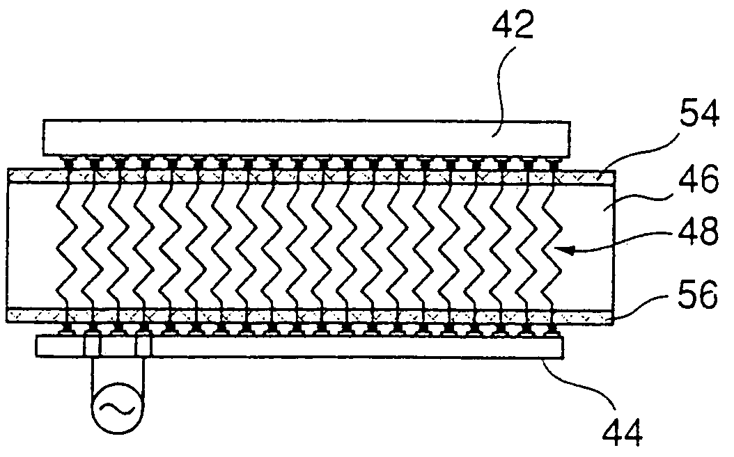
[0152]FIG. 23 shows a contactor 40 according to the sixth embodiment of the present invention. In FIG. 23, a contactor 40 is arranged between an electronic part 42 (an object to be contacted) such as an LSI and a test board 44 so as to electrically connect the electronic part 42 to the test board 44. The test board 44 is provided with a circuit for testing the electronic part 42, and the electronic part 42 is subjected to a burn-in test or a final test in a state where the electronic part 42 is connected to the test board 44 via the contactor 40.

[0153]The contactor 40 comprises a base 46 formed of an insulating material and a plurality of contact electrodes 48 which penetrate and extend through the base 46. The base 46 is formed in the shape of a plate, and has a surface 46a (first surface), which is arranged to face the electronic part 42, and a surface 46b (second surface), which is arranged ...


PUM


Abstract

A contactor has contact electrodes elastically deformable in a direction of thickness of the contactor so that the contactor can make a contact with a semiconductor device with an appropriate contact pressure. The contactor is positioned between the semiconductor device and a test board so as to electrically connect the semiconductor device to the test board. Each of a plurality of contact electrodes has a first contact electrode part, a second contact electrode part and a connecting part electrically connecting the first contact electrode part to the second contact electrode part. The first contact electrode part contacts an electrode of the semiconductor device. The second contact electrode part contacts a terminal of the test board. A combining member has an insulating characteristic and holds the connecting part of each of the contact electrodes in a predetermined arrangement.

Description

[0001]This application is a Divisional application of U.S. application Ser. No. 10 / 059,114, filed Jan. 31, 2002, now U.S. Pat. No. 6,791,345, and hereby entirely incorporated herein by reference.BACKGROUND OF THE INVENTION[0002]1. Field of the Invention[0003]The present invention generally relates to a contactor for electronic products and, more particularly, to a contactor for contacting electrodes of a semiconductor device to achieve a conductive connection so as to examine the semiconductor device such as a large-scale semiconductor integrated circuit (LSI) and a manufacturing method of such a contactor.[0004]In recent years, manufacturing technology of a semiconductor substrate or the like has accomplished remarkable development. In connection with the development, circuit patterns of semiconductor devices such as an LSI have been changed to a fine structure, and an increase in the number of terminals and miniaturization of terminals have also been progressed with remarkable spe...

Claims


Application Information

Patent Timeline
Patent Type & Authority Patents(United States)
IPC IPC(8): G01R31/26G01R1/067G01R1/073H01L21/66H01R33/76
CPCG01R1/06716G01R3/00G01R1/07357G01R1/06733
Inventor MARUYAMA, SHIGEYUKITASHIRO, KAZUHIROWATANABE, NAOYUKIKOIZUMI, DAISUKEHASHITANI, TAKAFUMIYANO, EI
Owner FUJITSU SEMICON LTD
Learn More