Method of manufacturing nonvolatile organic memory device and nonvolatile organic memory device manufactured by the same

a nonvolatile organic memory and organic technology, applied in solid-state devices, instruments, nanoinformatics, etc., can solve the problems of high cost of memory chips, disadvantages of conventional flash memory, and increase process costs, so as to achieve rapid and uniform dispersion

Active Publication Date: 2008-07-29
SAMSUNG ELECTRONICS CO LTD
View PDF5 Cites 21 Cited by
  • Summary
  • Abstract
  • Description
  • Claims
  • Application Information

AI Technical Summary

Benefits of technology

[0011]Accordingly, embodiments of the present invention have been made keeping in mind the above problems occurring in the related art, and an object of embodiments of the present invention is to provide a method of manufacturing a nonvolatile organic memory device, which method allows conductive nanoparticles to rapidly and uniformly disperse in an organic material using in-situ dispersion of an ionic solution of conductive nanoparticles.
[0012]Another object of embodiments of the present invention is to provide a method of manufacturing a nonvolatile organic memory device having environmentally friendly properties and a low operating voltage.

Problems solved by technology

However, conventional flash memory is disadvantageous because it has a limited number of recording / erasing times and a slow recording speed.
Further, in order to manufacture flash memory having a high memory capacity, line width per unit area should be decreased, which increases process costs resulting in high costs to manufacture memory chips.
Moreover, due to difficulties in chip manufacturing techniques it is difficult to further miniaturize the chips.
However, since the electroforming process cannot control the size or size distribution of metal particles, physical properties of the devices are inconsistent.
At this time, memory behavior, as well as the operating voltage and operating current of the memory device, varies and contributes to inconsistent device properties, which reduces the reproducibility and results in severely defective products.
As such, however, the nanoparticles may aggregate due to mutual attraction, losing the properties of nanoparticles.
To prevent aggregation of nanoparticles, although a process of encapsulating the nanoparticles is additionally performed between the synthesizing of nanoparticles and the blending of the synthesized nanoparticles with the polymer, such an encapsulation process suffers from a shortcoming of requiring several days or more.
In addition, the nanoparticles may aggregate again when being dispersed in the medium, and also, a large amount of solvent is used, thus causing environmental contamination problems.

Method used


Image

  • Method of manufacturing nonvolatile organic memory device and nonvolatile organic memory device manufactured by the same
  • Method of manufacturing nonvolatile organic memory device and nonvolatile organic memory device manufactured by the same
  • Method of manufacturing nonvolatile organic memory device and nonvolatile organic memory device manufactured by the same

Examples


example 1

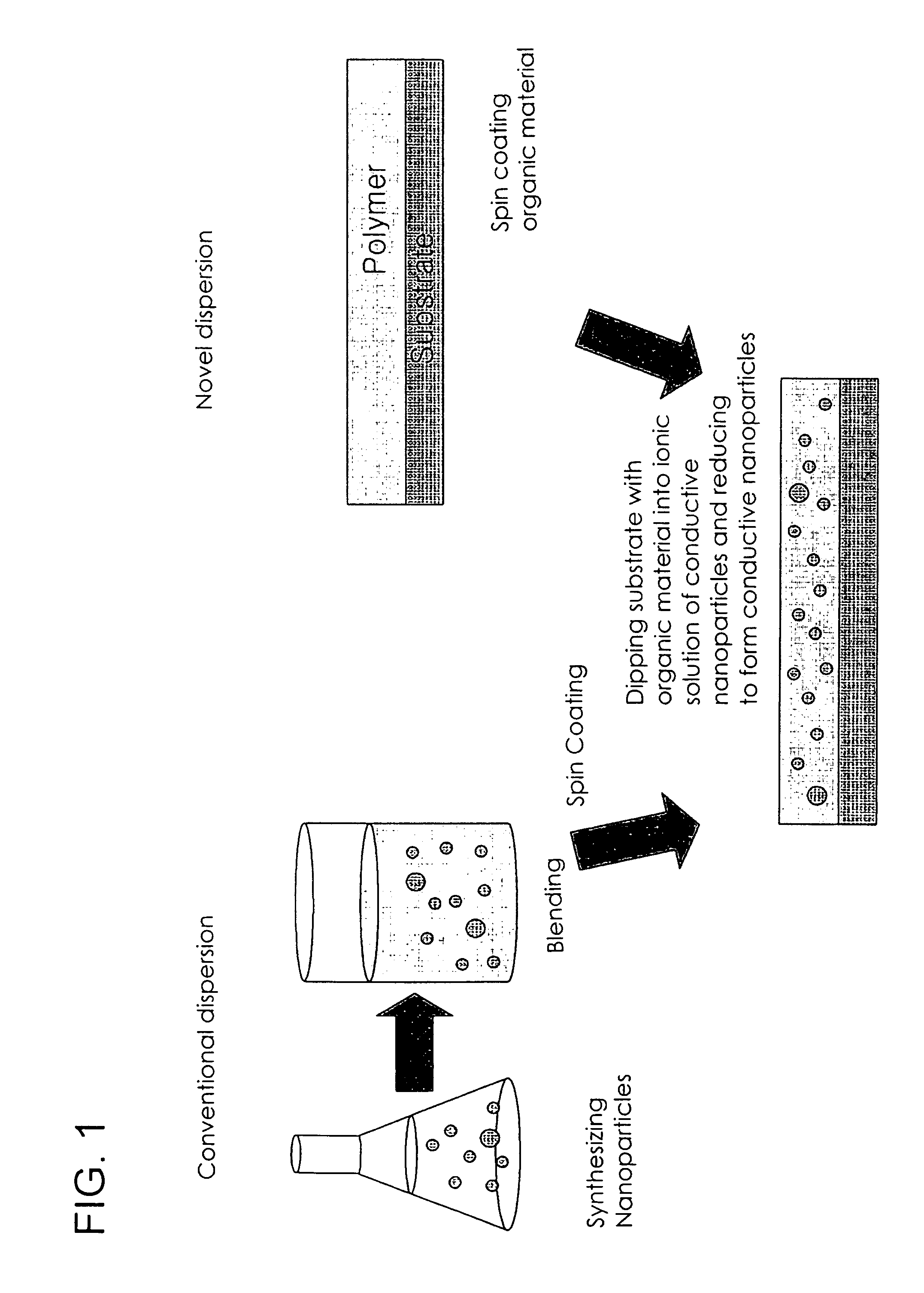
[0036]On a glass substrate having a lower electrode layer formed by depositing aluminum on the substrate, a solution of poly(styrene-b-vinylpyridine) (molecular weight of each block: 57,000) was spin coated and then baked at 120° C. for 20 min. The coated substrate was dipped into a 1 wt % HAuCl4 ethanol solution for about 1 min and washed several times with deionized water. Subsequently, the substrate was dipped into 1 wt % NaBH4 methanol solution for about 15 sec, washed several times with deionized water, and dried overnight at 60° C. in a vacuum atmosphere. Upon observing the surface of the dried substrate, the substrate was confirmed to be suitable for formation of another electrode layer from the result that the substrate was still flat, without being roughened by the solution. Thereafter, as an upper electrode layer, aluminum was deposited on the substrate using a thermal evaporation process, to manufacture a nonvolatile organic memory device. As such, the memory layer was 15...

example 2

[0038]On a glass substrate, aluminum was deposited using a thermal evaporation process to form a lower electrode layer, which was then spin coated with PMMA to form a 20 nm thick barrier layer. Subsequently, on the glass substrate having the barrier layer formed thereon, a solution of poly(styrene-b-vinylpyridine) (molecular weight of each block: 57,000) was spin coated and then baked at 120° C. for 20 min to form an organic material layer. The substrate coated with the organic material was dipped into a 1 wt % Au(PMe3)Me ethanol solution for about 1 min and washed several times with deionized water. Subsequently, the substrate was dipped into a 1 wt % NaBH4 methanol solution for about 15 sec, washed several times with deionized water, and dried overnight at 60° C. in a vacuum atmosphere. Then, as an upper electrode layer, aluminum was deposited on the substrate using a thermal evaporation process, to manufacture a nonvolatile organic memory device. As such, the memory layer was 15-...


PUM

PropertyMeasurementUnit
thicknessaaaaaaaaaa
thicknessaaaaaaaaaa
voltageaaaaaaaaaa

Abstract

A method of manufacturing a nonvolatile organic memory device including a memory layer interposed between an upper electrode layer and a lower electrode layer, which includes dispersing ions of conductive nanoparticles in an organic material disposed between the two electrode layers and then reducing the ions of conductive nanoparticles into conductive nanoparticles in the organic material to form a desired memory layer. In addition, a nonvolatile organic memory device manufactured by the method of the current invention is also provided. The method allows the memory device to be manufactured using a rapid, simple, and environmentally friendly process, without the need for an encapsulation process. As well, the memory device has a low operating voltage, and hence, is suitable for application to various portable electronic devices that must have low power consumption.

Description

BACKGROUND OF THE INVENTION[0001]This non-provisional application claims priority under 35 U.S.C. § 119(a) on Korean Patent Application No. 2004-111926 filed on Dec. 24, 2004, which is herein expressly incorporated by reference.[0002]1. Field of the Invention[0003]Embodiments of the present invention relate, generally, to a method of manufacturing a nonvolatile organic memory device and a nonvolatile organic memory device manufactured by the same. More particularly, embodiments of the present invention relate to a method of manufacturing a nonvolatile organic memory device, which is advantageous because it is environmentally friendly and has superior processability by dispersing ions of conductive nanoparticles in an organic material disposed between two electrode layers and reducing the ions of conductive nanoparticles into conductive nanoparticles in the organic material, and a nonvolatile organic memory device, having a low operating voltage, manufactured by such a method.[0004]2...

Claims


Application Information

Patent Timeline
Patent Type & Authority Patents(United States)
IPC IPC(8): H01L21/31H01L21/469
CPCB82Y10/00H01L21/02G11C13/0016G11C13/0014H10B99/00H01L21/20
Inventor KANG, YOON SOKLEE, SANG KYUNJOO, WON JAELEE, KWANG HEE
Owner SAMSUNG ELECTRONICS CO LTD
Why Eureka
Try Eureka