Methods to improve the operation of SOI devices

a technology of silicon on insulator and soi, applied in the field of integrated circuits, can solve the problems of lack of flexibility in the operation of an integrated circuit device, inability to function every day, and production of difficulties, and achieve the effect of enhancing the operation of soi fabricated devices, reducing the speed penalty for successive access to the memory subarray, and eliminating or greatly reducing the speed penalty

Inactive Publication Date: 2008-07-29
GLOBALFOUNDRIES INC
View PDF51 Cites 49 Cited by
  • Summary
  • Abstract
  • Description
  • Claims
  • Application Information

AI Technical Summary

Benefits of technology

[0019]According to the present invention, a circuit and methods for enhancing the operation of SOI fabricated devices are disclosed. In a preferred embodiment of the present invention, a pulse discharge circuit is provided. Here, a circuit is designed to do a pulse discharge that will eliminate the accumulated electrical charge on the SOI devices in the memor

Problems solved by technology

Indeed, in many ways, our everyday life could not function as it does without integrated circuits.
While providing many advantages, this dielectric isolation also produces some difficulties not encountered with more conventional integrated circuit devices.
Thus, the lack of flexibility in the operation of an integrated circuit device due to the SOI insulating region is often inconvenient.
This shift can adversely affect the operation of the circuit and introduce errors into the information being processed by the device.
In addition, thermal fluctuations can also cause electrical charges to accumulate in the body of the transistors.
For example, in synchronization circuits with critical timing requirements, the transistor may not switch on at the appropriate time and the circuit may not operate at all.
If subsequent accesses are to the same memory segment, no charge sufficient to c

Method used


Image

  • Methods to improve the operation of SOI devices
  • Methods to improve the operation of SOI devices
  • Methods to improve the operation of SOI devices

Examples


Embodiment Construction

[0030]The present invention relates to the use and operation of integrated circuit transistors, particularly SOI transistors. For those individuals who are not familiar with CMOS and SOI fabricated devices, the Overview section below presents some basic concepts that will help to understand the invention. Those who are skilled in the art may wish to skip this section and begin with the Detailed Description Section instead.

OVERVIEW

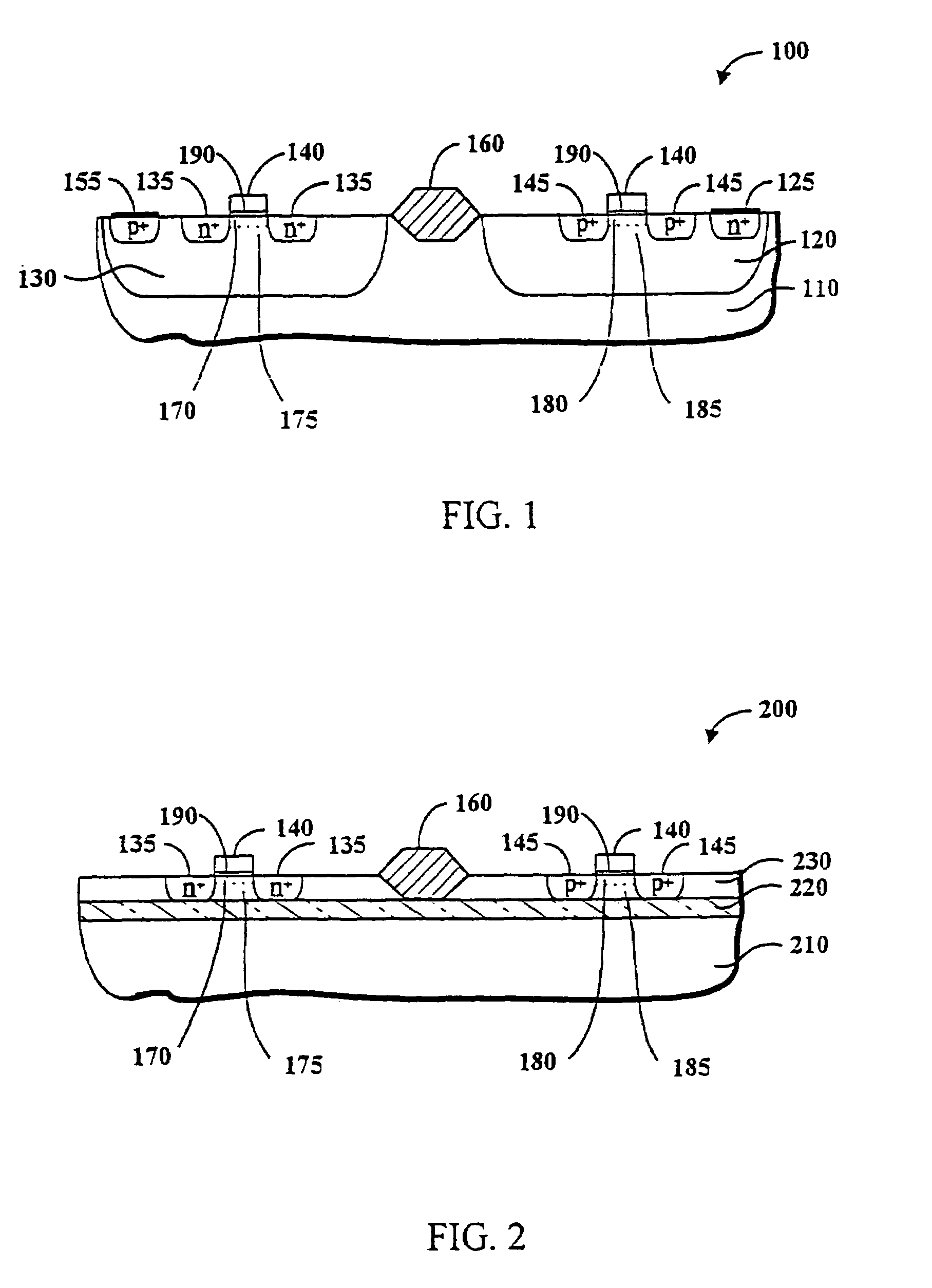
[0031]Referring now to FIG. 1, a portion of a typical bulk CMOS wafer 100 includes: a substrate 110; an n-well 120; an n-well contact 125; a p-well 130; n+ source and drain diffusions 135; polysilicon gate contacts 140; p+ source and drain diffusions 145; a p-well contact 155; a surface isolation 160; an n-channel 170; an n-body 175; a p-channel 180; a p-body 185, and a gate oxide 190.

[0032]The designation of a particular device as a p-channel device or an n-channel device depends on the type of fabrication process used to create the device. Substrate 110 i...


PUM


Abstract

According to the present invention, a circuit and methods for enhancing the operation of SOI fabricated devices are disclosed. In a preferred embodiment of the present invention, a pulse discharge circuit is provided. Here, a circuit is designed to provide a pulse that will discharge the accumulated electrical charge on the body of the SOI devices in the memory subarray just prior to the first access cycle. As explained above, once the accumulated charge has been dissipated, the speed penalty for successive accesses to the memory subarray is eliminated or greatly reduced. With a proper control signal, timing and sizing, this can be a very effective method to solve the problem associated with the SOI loading effect. Alternatively, instead of connecting the bodies of all SOI devices in a memory circuit to ground, the bodies of the N-channel FET pull-down devices of the local word line drivers can be selectively connected to a reference ground. This would enable the circuit to retain most of the speed advantages associated with SOI devices while overcoming the loading problem described above. With this preferred embodiment of the present invention, the major delay caused by the bipolar loading effect is minimized while the speed advantage due to providing a lower, variable Vt effect is preserved. The overall body resistance of the individual devices has a minimal effect on the device body potential.

Description

[0001]This application is a continuation of U.S. patent application Ser. No. 09 / 063,823, filed Apr. 22, 1998, which claims priority from U.S. provisional patent application Ser. No. 60 / 044,251 filed on Apr. 23, 1997, which is now U.S. Pat. No. 6,160,292 issued Dec. 12, 2000.BACKGROUND OF THE INVENTION [0002]1. Technical Field[0003]This invention generally relates to integrated circuits. More specifically, the present invention relates to enhancing the performance of Silicon On Insulator (SOI) devices.[0004]2. Background Art[0005]Today, our society is heavily dependent on high-tech electronic devices for everyday activity. Integrated circuits are the components that give life to our electronic devices. Integrated circuits are found in widespread use throughout our country, in appliances, in televisions and personal computers, and even in automobiles. Additionally, manufacturing and production facilities are becoming increasingly dependant on the use of integrated circuits for operati...

Claims


Application Information

Patent Timeline
IPC IPC(8): G11C5/14G11C16/08H01L27/12
CPCH01L27/1203G11C16/08
Inventor O'BRIEN, LEGAL REPRESENTATIVE, CATHERINEFLAKER, LEGAL REPRESENTATIVE, SCOTTFLAKER, LEGAL REPRESENTATIVE, SHIRLEY A.FLAKER, LEGAL REPRESENTATIVE, BRUCEFLAKER, LEGAL REPRESENTATIVE, ANNEFLAKER, LEGAL REPRESENTATIVE, HEATHERHSU, LOUIS L.KUANG, JENTE B.FLAKER, ROY CHILDS
Owner GLOBALFOUNDRIES INC
Why Eureka
Try Eureka