Display device and method of fabricating the same

a display device and display technology, applied in the field of semiconductor elements, to achieve the effect of reducing the number of masks, reducing the manufacturing cost, and reducing the manufacturing process

Inactive Publication Date: 2008-08-12
SEMICON ENERGY LAB CO LTD
View PDF131 Cites 25 Cited by
  • Summary
  • Abstract
  • Description
  • Claims
  • Application Information

AI Technical Summary

Benefits of technology

[0065]Further, means for resolving the second problem (hereinafter, referred to as second aspect of the invention) will be explained as follows in reference to FIGS. 21A and 21B. The second aspect of the invention is a light emitting device (specifically, EL display device) fabricated by the fabricating process preferable in embodying the first aspect of the invention and is an aspect of the invention characterized in that the fabricating process is reduced by reducing the number of laminated layers as a whole and fabricating cost is reduced as a result.
[0066]According to the structure shown by FIGS. 2A and 2B, since the pixel electrode is previously provided before forming the thin film transistor and therefore, it is not necessarily needed to provide a flattening film which is necessary when the pixel electrode is provided at a layer on an upper side of the thin film transistor (in FIGS. 2A and 2B, photosensitive organic resin film 961) as in an ordinary case. FIGS. 21A and 21B show a structure when the photosensitive organic resin film 961 is not provided. FIG. 21A shows a case in which the photosensitive organic resin film 961 of FIG. 2A is not provided and FIG. 21A shows a case in which the photosensitive organic resin film 961 of FIG. 2B is not provided. In FIG. 21A, notation 991 designates an insulating nitride film which is a third pa

Problems solved by technology

Further, it is a second problem thereof to provide a fabricating process preferable in reducing the number of steps of

Method used


Image

  • Display device and method of fabricating the same
  • Display device and method of fabricating the same
  • Display device and method of fabricating the same

Examples


embodiment 1

[0089]According to the embodiment, an explanation will be given of an example of making a position of forming the first opening portion 110 in FIGS. 3A and 3B differ therefrom in reference to FIGS. 10A and 10B. Further, FIGS. 10A and 10B show a sectional structure at a time point of forming a second opening portion. Further, notations used in FIGS. 3A and 3B are referred as necessary.

[0090]In FIG. 10A, notation 801 designates a first opening portion having a diameter φ1 and notation 802 designates a second opening portion having a diameter φ2. A characteristic of FIG. 10A resides in that the first opening portion 801 is provided to extrude from an end portion of the source region 103. The photosensitive organic resin film 109 can be formed at a position as shown by the embodiment since progress of etching is stopped by constituting an etching stopper by the first passivation film 108. Further, the structure can be constituted similarly not only at a portion in contact with the sourc...

embodiment 2

[0093]According to the embodiment, there is shown an example of using a bottom gate type thin film transistor (specifically, inverse stagger type TFT) as a thin film transistor in embodying the first aspect of the invention or the second aspect of the invention, that is, an example of using an inverse stagger type TFT as a switching TFT and a driving TFT in embodying the light emitting device shown in FIGS. 1A and 1B.

[0094]The embodiment will be explained in reference to FIG. 11. In FIG. 11A, notation 301 designates a substrate, notation 302 designates a gate electrode, notation 303 designates a gate insulating film, notation 304 designates a source region, notation 305 designates a drain region, notations 306a and 306b designate LDD regions, notation 307 designates a channel forming region and these are constituted by using a semiconductor film provided above the gate insulating film provided to cover the gate electrode 302. Further, notations 308 and 309 designate inorganic insula...

embodiment 3

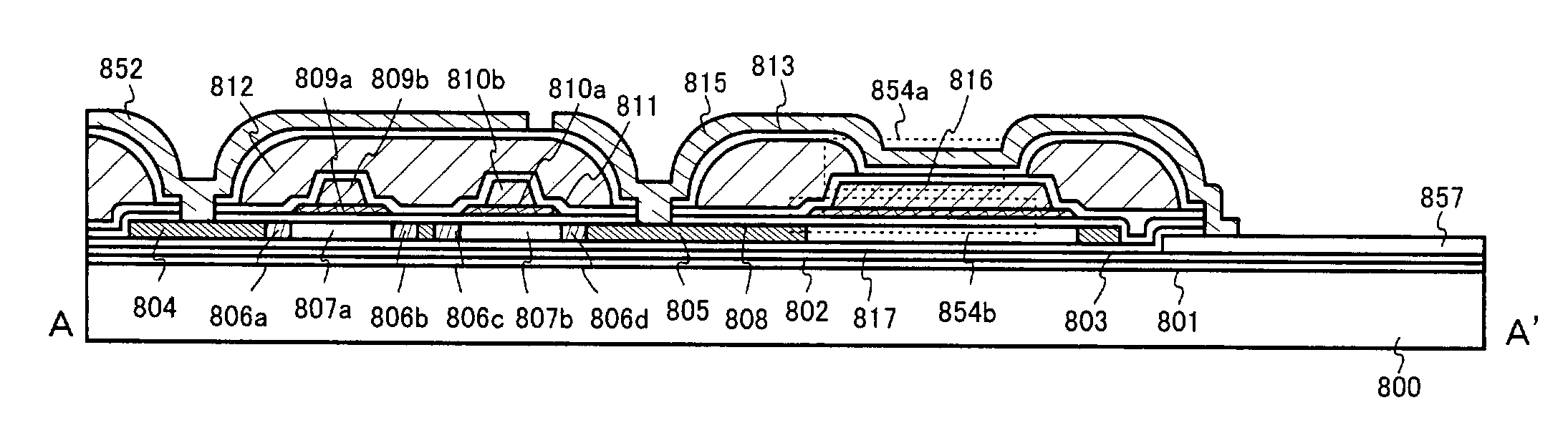
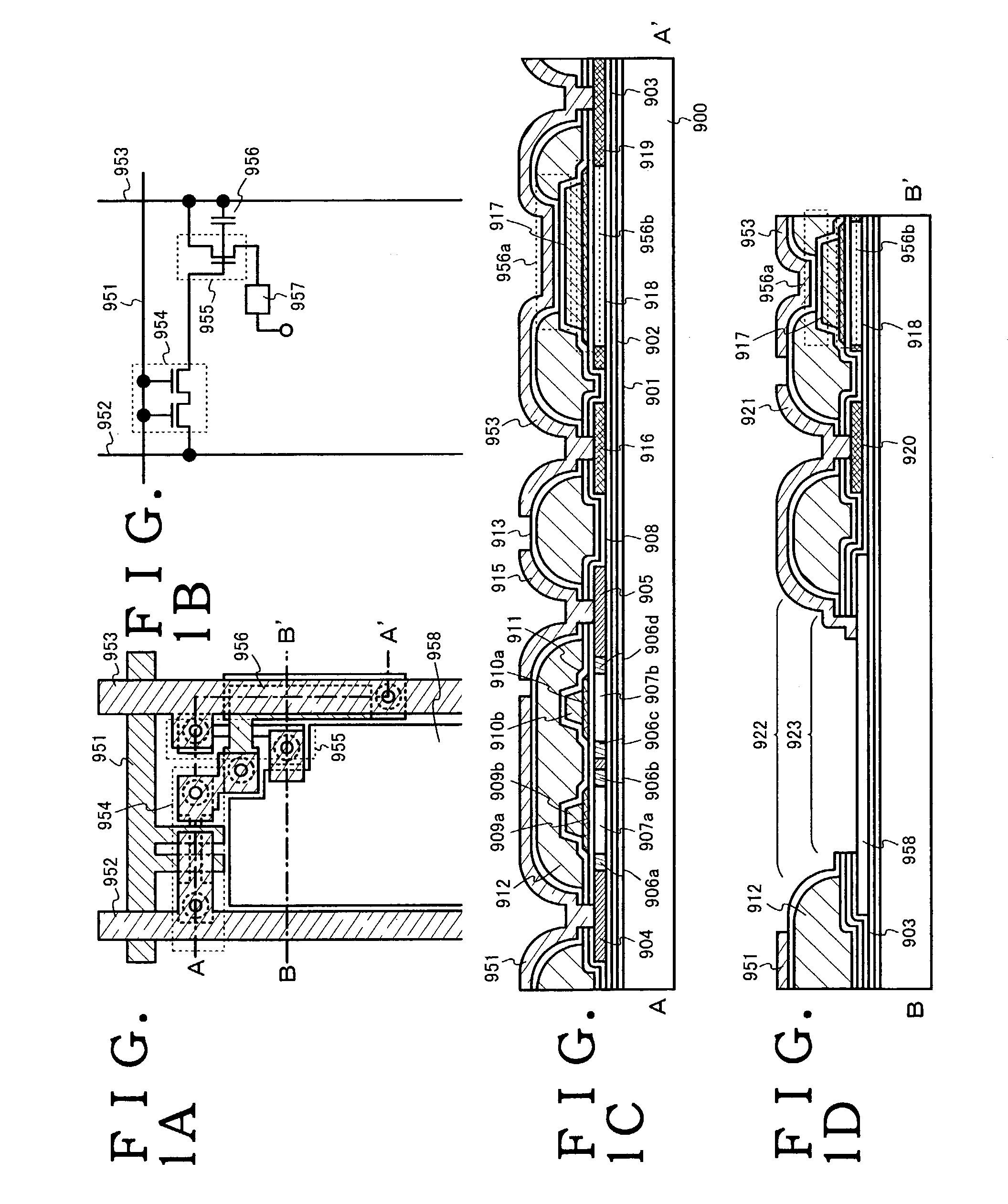
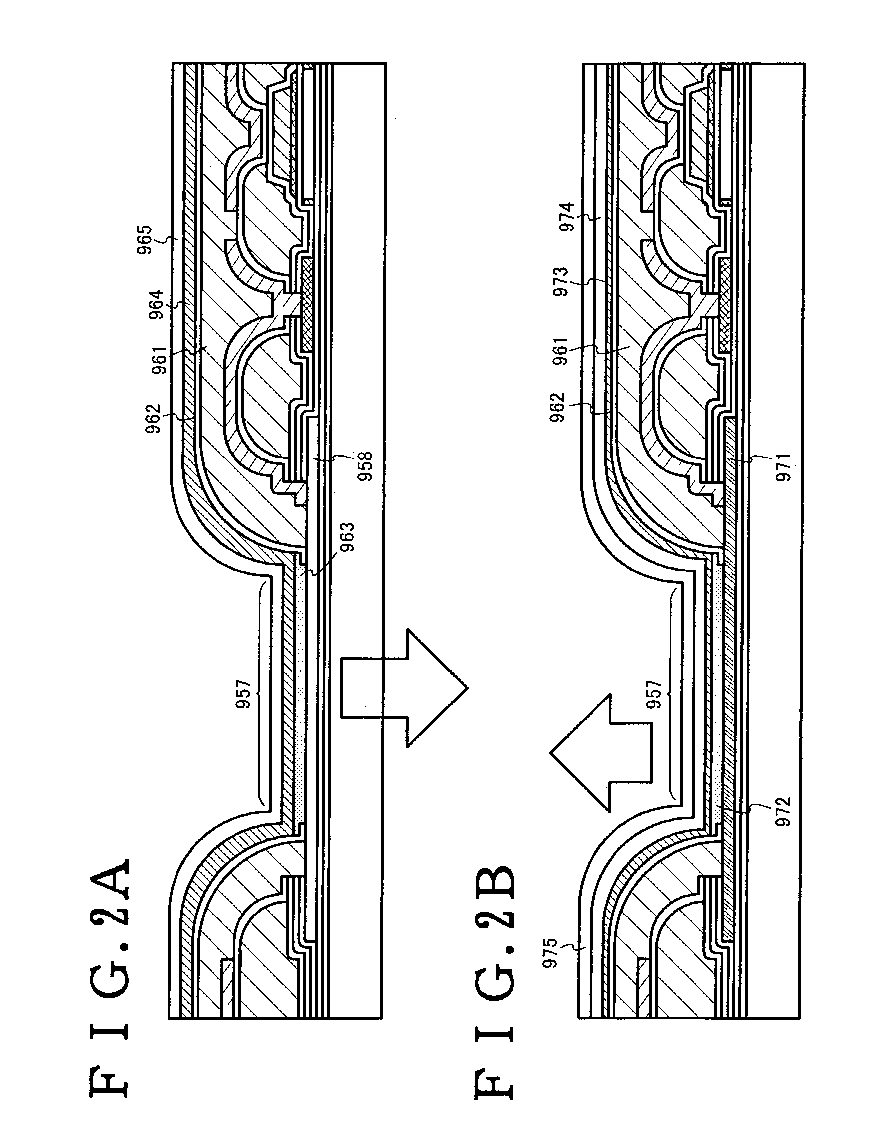
[0098]According to the embodiment, an explanation will be given of an example in which the first aspect of the invention or the second aspect of the invention is applied to a liquid crystal display device. In FIGS. 12A, 12B, 12C and 12D, FIG. 12A is a top view at a pixel of a liquid crystal display device (however, up to forming a pixel electrode), FIG. 12B is a circuit diagram thereof and FIGS. 12C and 12D are sectional views taken along a line A-A′ and a line B-B′ of FIG. 12A.

[0099]As shown by FIGS. 12A and 12B, a display portion of the liquid crystal display device includes a plurality of pixels surrounded by gate wiring 851 and a data wiring 852 in a matrix arrangement and each of the pixels is provided with TFT functioning as a switching element (hereinafter, referred to as switching TFT) 853, a capacitor portion 854 and a liquid crystal element 855. Further, although the liquid crystal element 855 is not illustrated in FIG. 2A, the liquid crystal element 855 can be formed by p...


PUM


Abstract

To achieve promotion of stability of operational function of display device and enlargement of design margin in circuit design, in a display device including a pixel portion having a semiconductor element and a plurality of pixels provided with pixel electrodes connected to the semiconductor element on a substrate, the semiconductor element includes a photosensitive organic resin film as an interlayer insulating film, an inner wall face of a first opening portion provided at the photosensitive organic resin film is covered by a second insulating nitride film, a second opening portion provided at an inorganic insulating film is provided on an inner side of the first opening portion, the semiconductor and a wiring are connected through the first opening portion and the second opening portion and the pixel electrode is provided at a layer on a lower side of an activation layer.

Description

BACKGROUND OF THE INVENTION[0001]1. Field of the Invention[0002]The present invention relates to a semiconductor element (typically, a transistor) and a manufacturing method thereof, and more specifically belongs to a technique of a display device using a thin film transistor as a device. That is, the present invention belongs to a technique concerning a display device represented by a liquid crystal display device, an electroluminescence display device, or the like, a technique concerning a sensor represented by a CMOS sensor or the like, and other techniques concerning various semiconductor devices in which a semiconductor integrated circuit is mounted.[0003]2. Description of the Related Art[0004]In recent years, the development for a liquid crystal display device and an electroluminescence display device in which thin film transistors (TFTs) are integrated on a glass substrate has been progressed. These display devices each are one of semiconductor devices characterized in that t...

Claims


Application Information

Patent Timeline
IPC IPC(8): H01L31/036G02F1/1368G09F9/30H01L21/336H01L21/77H01L21/84H01L27/12H01L29/786H01L51/50H05B33/14
CPCH01L27/12H01L29/78621H01L33/44H01L27/1248H01L27/1288H01L2924/0002H01L2924/00H01L29/78
Inventor HAYAKAWA, MASAHIKOMURAKAMI, SATOSHIYAMAZAKI, SHUNPEIAKIMOTO, KENGO
Owner SEMICON ENERGY LAB CO LTD
Why Eureka
Try Eureka