
Hierarchical feature extraction for electrical interaction

a technology of electrical interaction and feature extraction, applied in the direction of electric digital data processing, instruments, computing, etc., can solve the problems of large amount of memory and computer time to analyze, and the circuit as designed on the computer will not perform as anticipated

Inactive Publication Date: 2008-08-12
SIEMENS PROD LIFECYCLE MANAGEMENT SOFTWARE INC
View PDF18 Cites 12 Cited by
  • Summary
  • Abstract
  • Description
  • Claims
  • Application Information

AI Technical Summary

Benefits of technology

This approach significantly reduces the time required to model electrical interactions in integrated circuit designs by minimizing redundant calculations and optimizing memory usage, enabling more efficient verification and design adjustments.

Problems solved by technology

In many instances, a circuit as designed on a computer will not perform as anticipated due to capacitances that occur between the physical microelectronic elements that comprise the circuit as well as the small but measurable resistance of these elements.
However, such an approach can create extremely large files and therefore require a large amount of memory and computer time to analyze.

Method used

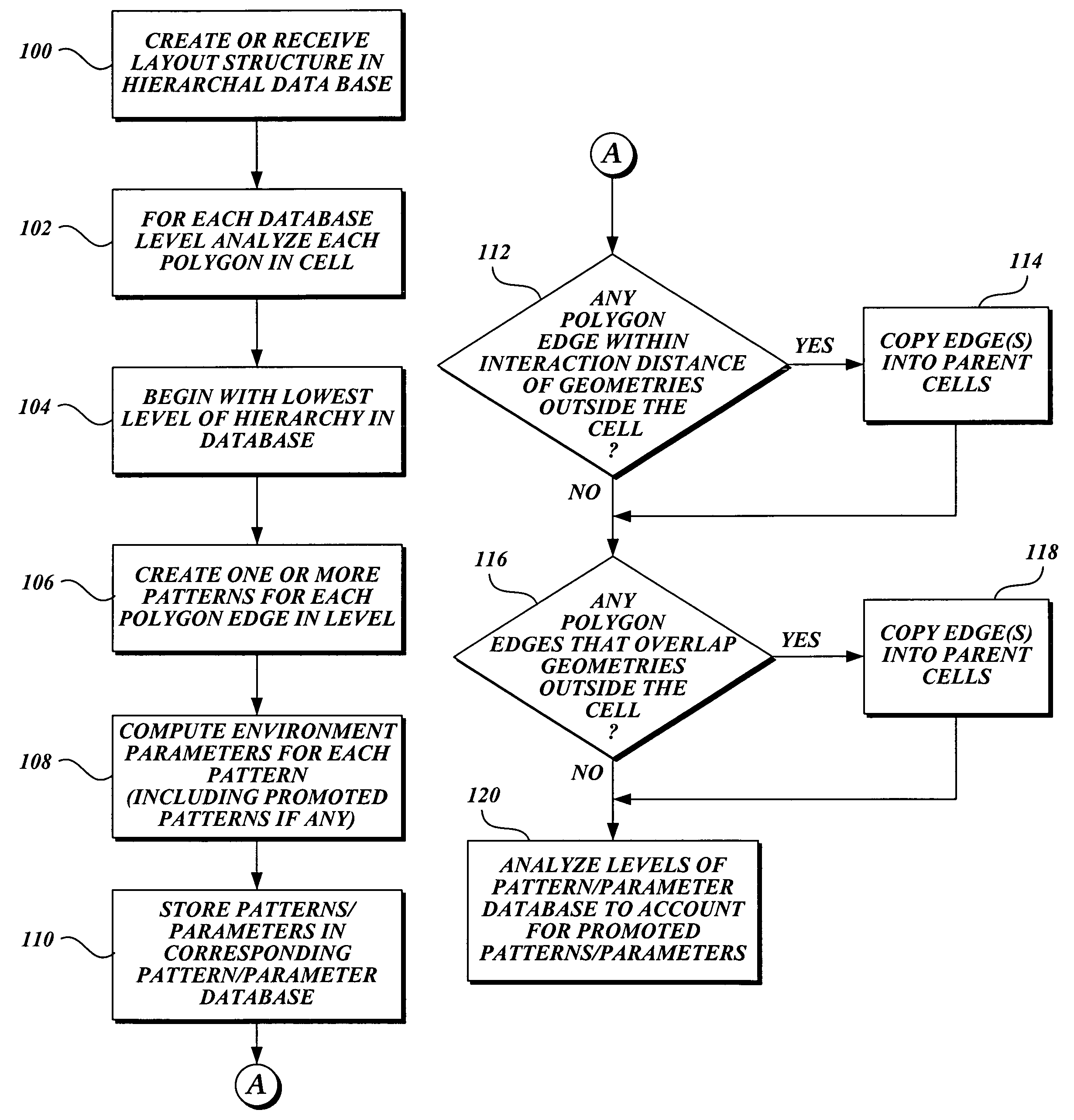

Image

  • Hierarchical feature extraction for electrical interaction
  • Hierarchical feature extraction for electrical interaction
  • Hierarchical feature extraction for electrical interaction

Examples


Embodiment Construction

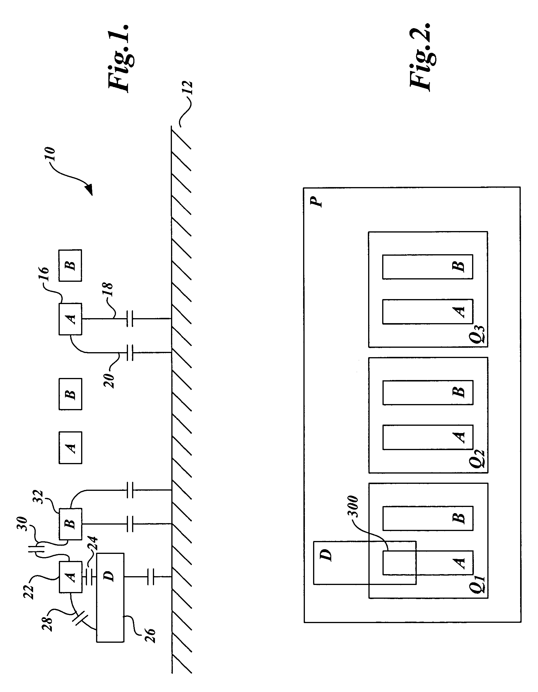
[0020]FIG. 1 is a simplified representation of a cross-section of a portion of an integrated circuit. An integrated circuit 10 includes a substrate 12 and a number of conductive circuit elements formed in layers above the substrate 12. Many of the features or elements, such as those labeled A and B are repeated in the integrated circuit. Other elements, such as that labeled D, may appear only once in the circuit layout.

[0021]As will be appreciated by those skilled in the art of circuit design and modeling, capacitances may be created between the circuit elements due to their area and the physical proximity to one another. When not blocked by an intervening element, each element in the circuit may have a plate capacitance between it and the substrate 12. For example, element 16 has a plate capacitance 18 that can be modeled as a capacitor connected between the lower surface of the element 16 and the substrate 12. In addition, the vertical edges of each element create fringe capacitan...


PUM


Abstract

A method of calculating electrical interactions of circuit elements in an integrated circuit layout without flattening the entire database that describes the layout. In one embodiment, a hierarchical database is analyzed and resistance and capacitance calculations made for a repeating pattern of elements are re-used at each instance of the repeated pattern and adjusted for local conditions. In another embodiment, a circuit layout is converted into a number of tiles, wherein the resistance and capacitance calculations made for the circuit elements in the center and a boundary region of the tiles are computed separately and combined. Environmental information that affects electrical interaction between circuit elements in different levels of hierarchy is calculated at a lower level of hierarchy so that such calculations do not need to be made for each placement of a repeated cell and so that not all interacting elements need to be promoted to the same hierarchy level to compute the electrical interactions.

Description

CROSS-REFERENCE(S) TO RELATED APPLICATION(S)[0001]The present application is a divisional of U.S. patent application Ser. No. 10 / 180,956 (now U.S. Pat. No. 6,931,613), filed Jun. 24, 2002, the benefit of which is claimed under 35 U.S.C. §120.FIELD OF THE INVENTION[0002]The present invention relates to verification techniques for integrated circuit designs.BACKGROUND OF THE INVENTION[0003]In the field of semiconductor manufacturing, physical descriptions of microdevice layouts are generally represented using data formats such as GDSII. In this representation, individual circuit elements are represented by polygons, which are typically described as a sequence of vertices. The circuit elements placed in the various physical layers in the device are represented by data layers in the description. related groups of device elements on various layers can be combined in a description of a subset of the layout, often called a cell. In turn, cells can contain other, smaller cells, or be contai...

Claims


Application Information

Patent Timeline
Patent Type & Authority Patents(United States)
IPC IPC(8): G06F17/50G06F9/45
CPCG06F17/5081G06F17/5036G06F30/367G06F30/398
Inventor KAUTH, THOMAS H.GIBSON, PATRICK D.HERTZ, KURT C.GRODD, LAURENCE W.
Owner SIEMENS PROD LIFECYCLE MANAGEMENT SOFTWARE INC
Learn More