Non-contact method and apparatus for measurement of leakage current of p-n junctions in IC product wafers

Inactive Publication Date: 2008-08-19
AHBEE 1
View PDF7 Cites 24 Cited by
  • Summary
  • Abstract
  • Description
  • Claims
  • Application Information

AI Technical Summary

Benefits of technology

[0009]The present invention also provides a means for increasing the accuracy and versatility of the measurement through several methods; providing a means for checking and adjusting the air gap separation between the probe electrodes and the p-n-junction to establish uniform and known capacitive coupling o

Problems solved by technology

As the number of transistors per IC increases, the contribution to dynamic and standby power drains from transistor junction leakage curren

Method used


Image

  • Non-contact method and apparatus for measurement of leakage current of p-n junctions in IC product wafers
  • Non-contact method and apparatus for measurement of leakage current of p-n junctions in IC product wafers
  • Non-contact method and apparatus for measurement of leakage current of p-n junctions in IC product wafers

Examples


Embodiment Construction

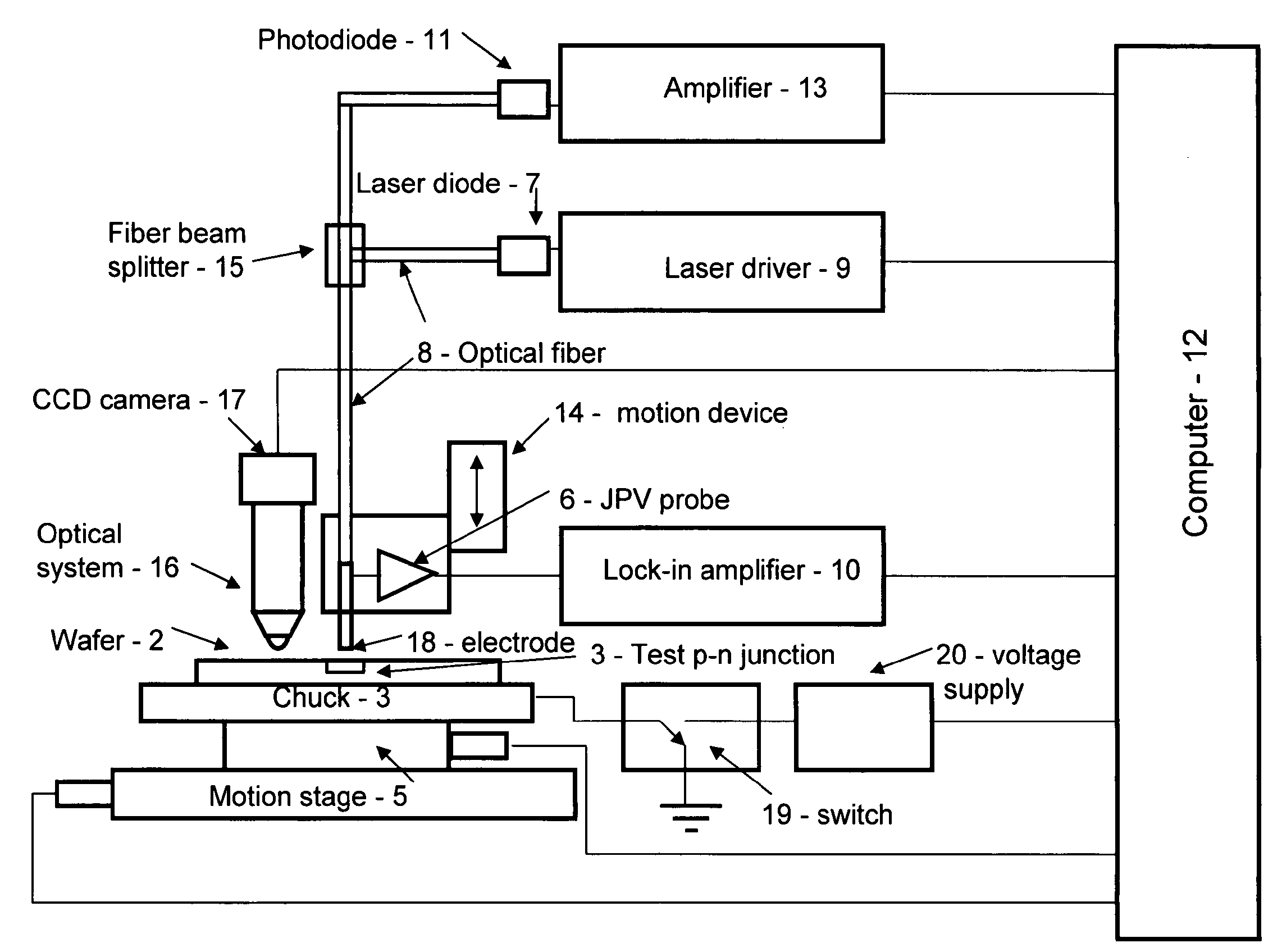
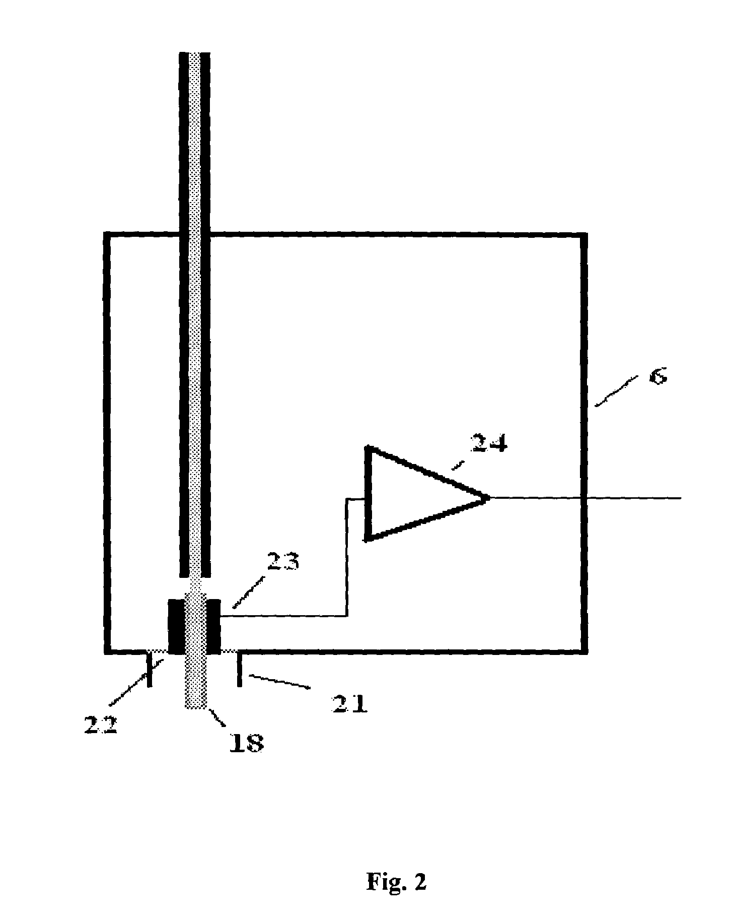
[0015]In FIG. 1, a non-contact leakage current apparatus 1 is shown. A wafer 2, containing product IC devices and a test p-n junction 3, is located on a wafer chuck 4. The wafer chuck is placed on a precision motion stage 5. The apparatus comprises a probe 6 for leakage current (L) measurement. An electrode 18 is placed close to the junction surface 3 and is optically coupled to a modulated light source 7, connected to a driver supply 9, through an optical fiber 8. The electrical output of the PV probe 6 is connected to a signal demodulator or lock-in amplifier 10. Signal demodulator 10 and motors of the stage 5 are electrically connected to an interface and a computer 12. The air gap distance between the probe electrode 18 and the p-n junction 3 is controlled through a vertical motion control device 14 to establish a known and uniform capacitive coupling for the JPV signal. The electrical gain of the probe 6 can also be controlled without adjustment of the probe-to-junction gap by ...


PUM


Abstract

A non-contact apparatus and method for measuring of the leakage current and capacitance of p-n junctions in test structures within scribe lanes of IC product wafers is disclosed. The apparatus has a light source optically coupled with a fiber to a transparent electrode at the end of the fiber, which is brought close to the p-n junction under test. The ac signal generated from the test p-n junction is captured by this transparent and conducting coating electrode. The leakage current of a test p-n junction is determined using the frequency dependence of junction photo-voltage signal and reference signals from a p-n junction with low leakage current and known capacitance.

Description

BACKGROUND OF THE INVENTION[0001]The present invention relates to the non-contact measurement of leakage current of p-n junctions in test structures located in the scribe lanes of IC product wafers using a junction photo-voltage (JPV) technique[0002]As the number of transistors per IC increases, the contribution to dynamic and standby power drains from transistor junction leakage currents poses increasing limitations to the implementation of advanced technology designs and a serious power drain for battery-powered systems. Many process factors associated with the fabrication of ultra-shallow junctions (USJ), with junction depths less than 30 nm, contribute to the increasing junction leakage current density as transistor size is scaled to smaller dimensions. Monitoring junction leakage current on in-process IC product wafers provides timely input for tuning manufacturing conditions to minimize leakage current levels.[0003]The present invention provides a method and apparatus for non-...

Claims


Application Information

Patent Timeline
IPC IPC(8): G01R31/08G01R31/26
CPCG01R31/311
Inventor FAIFER, VLADIMIRCURRENT, MICHAELWONG, TIMOTHY
Owner AHBEE 1
Why Eureka
Try Eureka