External power ring with multiple tapings to reduce IR drop in integrated circuit

a technology of integrated circuits and power rings, applied in the field of very large scale integration (vlsi) integrated circuits, can solve the problems of ic failure, undesirable ir drop becomes even more serious in low-voltage supply applications, and extreme high operating speed with a large number of i/o signal interfaces, etc., to achieve significant reduction of distances from core logic, increase the associated coupling capacitance, and reduce detrimental ir drop

Active Publication Date: 2008-08-26
VIA TECH INC
View PDF13 Cites 6 Cited by
  • Summary
  • Abstract
  • Description
  • Claims
  • Application Information

AI Technical Summary

Benefits of technology

[0007]Accordingly, it is an object of the invention to reduce undesirable IR drops at the core of an integrated circuit. Furthermore, it is an object of the invention to reduce IR drops while not occupying more interface pins. Furthermore, it is an object of the invention to reduce IR drops while not deteriorating the performance of the integrated circuit.
[0009]In another embodiment of the invention, a power bus is provided as a grid of intersecting conductive traces. Through this grid, distances to core logic are significantly decreased and, therefore, detrimental IR drops are also significantly reduced. In another embodiment of the invention, positive and negative power busses are provided on different levels of a multiple metal layer IC. In providing negative and positive power busses on different layers, another embodiment of the invention, configures such busses as parallel traces so as to increase the associated coupling capacitance. This increased coupling capacitance improves the integrity of the power delivered to the integrated circuit by minimizing the effects of noise on the power supply. Still another embodiment of the invention, provides the power busses on the lowest levels of a multiple metal layer integrated circuit. By providing the power busses at the lower levels, shorts and other damage that can occur during a wire bonding process are avoided because the concentrated pressures associated with wire bonding are worst near the top layers, but sparsely distributed at the lower layers.
[0010]The present disclosure provides an integrated circuit having an improved power bus with reduced IR drops in the supply power to the integrated circuit. Moreover, the present invention provides a power bus that reduces noise on the power bus itself. Advantageously, manufacturability, testability and reliability are not compromised in the power bus of the present invention. These and other advantages will be clear upon understanding of the drawings and detailed description below.

Problems solved by technology

Most ICs with a large number of transistors and extremely high operating speed with a large count of I / O signal interfaces are subject to core power supply voltage IR drops, if they are not handled and measured properly.
Moreover, undesirable IR drops become even more serious in low-voltage supply applications.
For example, where an IC is operating at 1.8 volts, even a small IR drop can cause the IC to fail.
Then, even a noisy power supply can cause the IC to fail for such a low operating voltage.

Method used


Image

  • External power ring with multiple tapings to reduce IR drop in integrated circuit
  • External power ring with multiple tapings to reduce IR drop in integrated circuit
  • External power ring with multiple tapings to reduce IR drop in integrated circuit

Examples


Embodiment Construction

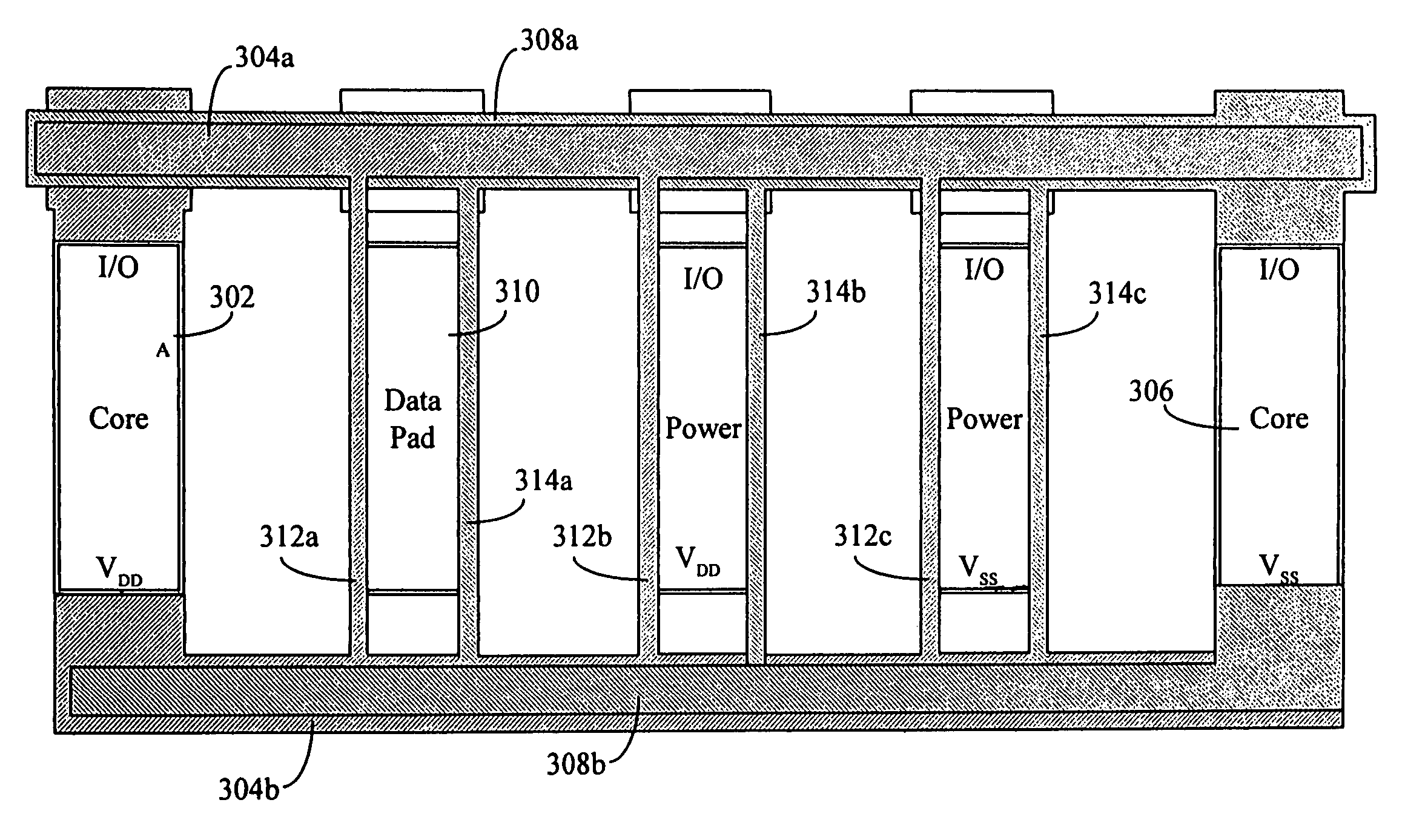
[0017]A. Development of VLSI Technology

[0018]New microprocessors, sometimes called central processing units (CPUs) are continually being developed with higher clock frequencies and increased functionality. Illustratively, reduced instruction set computing (RISC) architectures introduced complexities into interconnect and packaging systems where the input / output (I / O) timing issues at high clock frequencies need to be addressed. Dynamic random-access memory (DRAM), static random-access memory (SRAM), and electrically programmable read-only memory (EPROM) devices with increasing memory capacity and decreasing data access times are keeping pace with the rapid microprocessor development. In large part, it has been these microprocessors and memories that have driven IC device technologies. The rate of introduction of these IC components has increased over recent years as competition between manufacturers intensifies. Early introduction of new IC products enables system manufacturers to e...


PUM


Abstract

A power bus for use in an IC is disclosed that is configured as a grid and further formed using strips formed on I / O pads such as data I / O and multi-level voltage I / O pads. An IC is disclosed comprising a power supply I / O pad and a data I / O pad which are made of a deposited conductor. The power supply I / O pad is connected to a power bus and the data I / O pad is connected to circuitry. A strip of deposited conductor is formed closely adjacent to the data I / O pad wherein the strip is connected to the power bus. Parallel paths are developed within the integrated circuit to distribute power within the circuit. A similar approach is taken with respect to multi-level I / O pads. The power bus provide for reduced IR drops and better power supplies to core logic within an integrated circuit.

Description

FIELD OF THE INVENTION[0001]The present invention relates to the field of very large scale integration (VLSI) integrated circuits (ICs). More particularly, the present invention relates to a manner for providing power busses to an IC while reducing IR drops in a core of the IC.BACKGROUND OF THE INVENTION[0002]Complementary Metal Oxide Silicon (CMOS) technology has played an increasingly important role in the integrated circuit (IC) industry. Over the years, the technology has improved to the point that CMOS technology clearly holds center stage as the dominant VLSI technology. CMOS VLSI technology provides a large number of transistors and input / output (I / O) interfaces on an IC, sometimes called a chip, with extremely high operating speed. These advances in CMOS VLSI technology and especially in fabrication and manufacturing technologies have been driven by the reduction and downsizing of device dimensions.[0003]A number of enhancements may be added to the CMOS processes, primarily ...

Claims


Application Information

Patent Timeline
Patent Type & Authority Patents(United States)
IPC IPC(8): H01L23/48H01L27/10H01L23/522H01L23/528H01L27/02
CPCH01L23/5222H01L23/5286H01L27/02H01L24/06H01L2924/1305H01L2924/00H01L2224/02166H01L2224/05093H01L2924/14
Inventor LI, KEN-MINGABDEL-HAFEEZ, SALEH M.
Owner VIA TECH INC
Why Eureka
Try Eureka