Method of making a semiconductor chip assembly with a metal containment wall and a solder terminal

a technology of semiconductor chip and solder terminal, which is applied in the direction of printed circuit, sustainable manufacturing/processing, final product manufacturing, etc., can solve the problems of not avoiding the solder ball separation problem, the bga package becomes degraded or inoperable, etc., and achieves convenient manufacturing, reduced contact area, and enhanced mechanical support and protection of the routing line

Inactive Publication Date: 2008-09-02
BRIDGE SEMICON
View PDF158 Cites 13 Cited by
  • Summary
  • Abstract
  • Description
  • Claims
  • Application Information

AI Technical Summary

Benefits of technology

[0064]An advantage of the present invention is that the semiconductor chip assembly can be manufactured conveniently and cost effectively. Another advantage is that the encapsulant can be provided before the metal base is etched to reduce contact area between the metal base and the metal containment wall, thereby enhancing mechanical support and protection for the routing line. Another advantage is that the metal pillar can be formed by etching (subtractively) rather than by electroplating or electroless plating (additively) which improves uniformity and reduces manufacturing time and cost. Another advantage is that the solder terminal can extend into the metal containment wall within the insulative base rather than contact the assembly at a high-stress boundary in a lateral plane where an exposed major surface faces in the second direction, thereby reducing solder separation and improving reliability. Another advantage is that the connection joint can be made from a wide variety of materials and processes, thereby making advantageous use of mature connection joint technologies in a unique and improved manufacturing approach. Another advantage is that the assembly need not include wire bonds or TAB leads, although the process is flexible enough to accommodate these techniques if desired. Another advantage is that the assembly can be manufactured using low temperature processes which reduces stress and improves reliability. A further advantage is that the assembly can be manufactured using well-controlled processes which can be easily implemented by circuit board, lead frame and tape manufacturers. Still another advantage is that the assembly can be manufactured using materials that are compatible with copper chip and lead-free environmental requirements.

Problems solved by technology

Since the solder balls are contact terminals to the next level assembly, the BGA package becomes degraded or inoperative when the solder balls separate from the land metal elements.
For instance, sequentially plating nickel and gold films on a smooth and flat surface of a land metal element allows the solder ball to be easily fused to the land metal element, however this does not avoid the solder ball separation problem.

Method used


Image

  • Method of making a semiconductor chip assembly with a metal containment wall and a solder terminal
  • Method of making a semiconductor chip assembly with a metal containment wall and a solder terminal
  • Method of making a semiconductor chip assembly with a metal containment wall and a solder terminal

Examples


Embodiment Construction

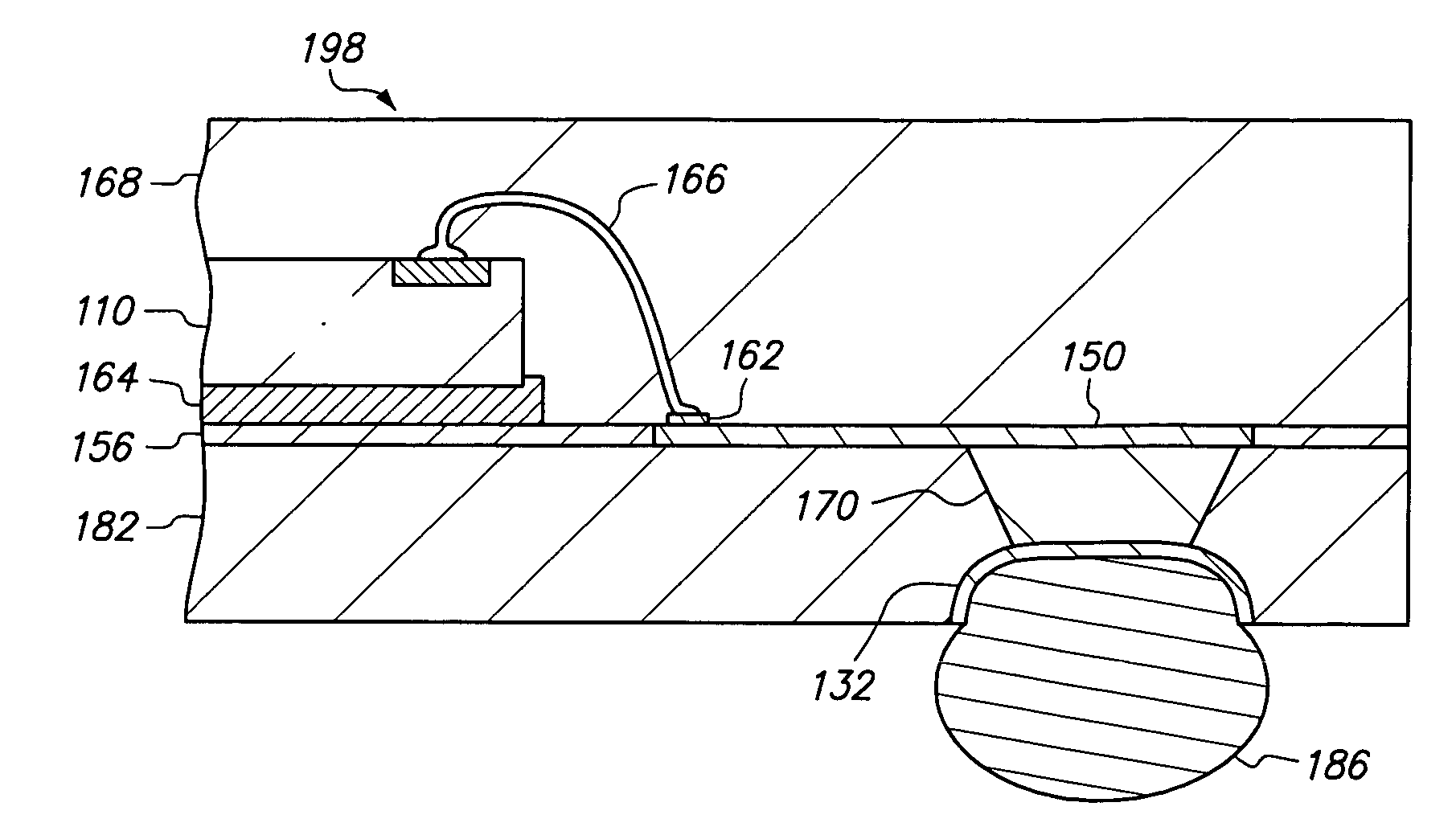
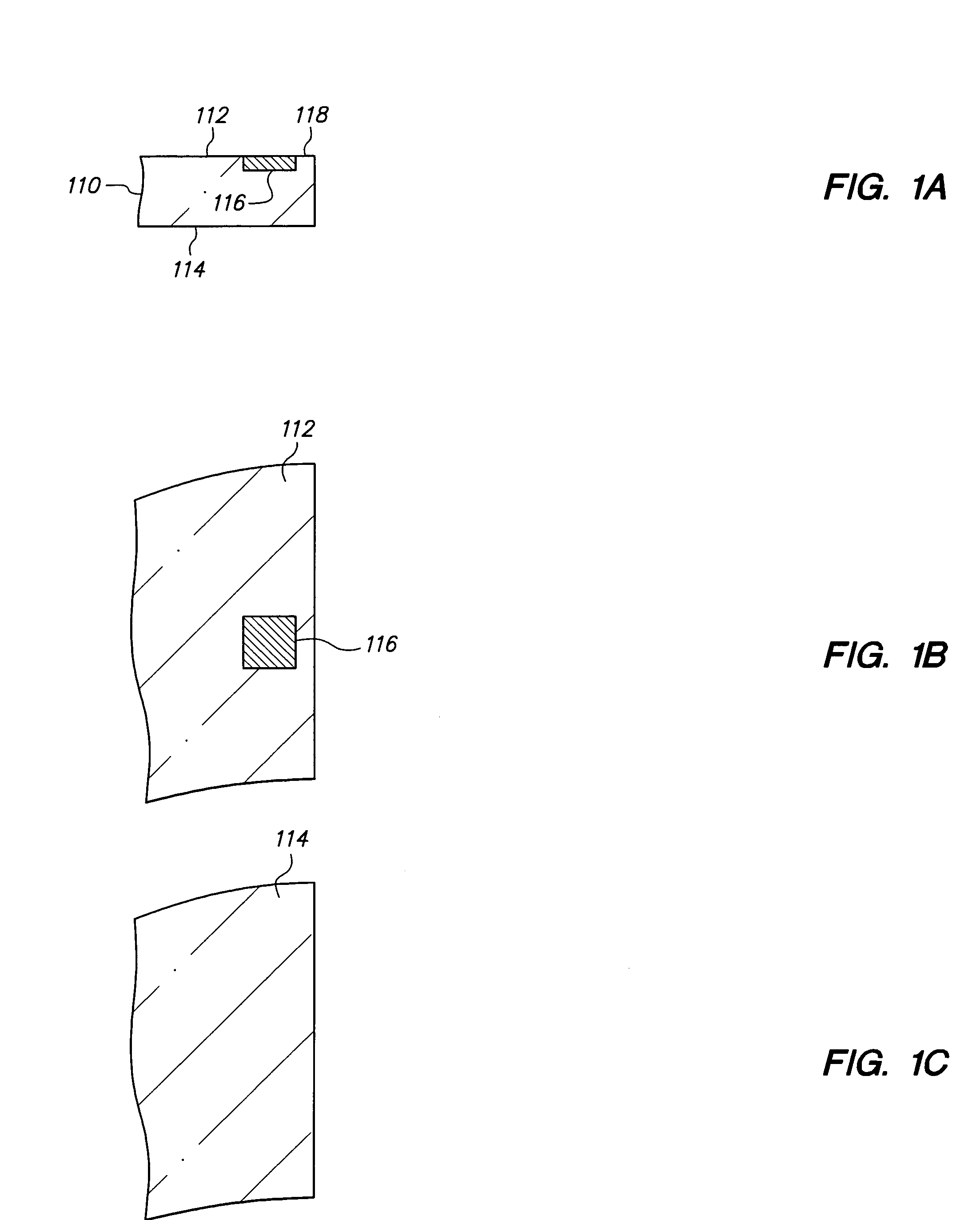
[0089]FIGS. 1A-27A, 1B-27B and 1C-27C are cross-sectional, top and bottom views, respectively, of a method of making a semiconductor chip assembly in accordance with a first embodiment of the present invention.

[0090]FIGS. 1A, 1B and 1C are cross-sectional, top and bottom views, respectively, of semiconductor chip 110 which is an integrated circuit in which various transistors, circuits, interconnect lines and the like are formed (not shown). Chip 110 includes opposing major surfaces 112 and 114 and has a thickness (between surfaces 112 and 114) of 150 microns. Surface 112 is the active surface and includes conductive pad 116 and passivation layer 118.

[0091]Pad 116 is substantially aligned with passivation layer 118 so that surface 112 is essentially flat. Alternatively, if desired, pad 116 can extend above or be recessed below passivation layer 118. Pad 116 provides a bonding site to electrically couple chip 110 with external circuitry. Thus, pad 116 can be an input / output pad or a ...


PUM


Abstract

A method of making a semiconductor chip assembly includes providing a metal base, a routing line, a metal containment wall and a solder layer in which the metal containment wall includes a cavity and the solder terminal contacts the metal containment wall in the cavity, mechanically attaching a semiconductor chip to the routing line, forming a connection joint that electrically connects the routing line and the pad, etching the metal base to reduce contact area between the metal base and the routing line and between the metal base and the metal containment wall, and providing a solder terminal that includes the solder layer.

Description

CROSS-REFERENCE TO RELATED APPLICATIONS[0001]This application is a continuation of U.S. application Ser. No. 11 / 213,398 filed Aug. 26, 2005, which is a continuation-in-part of U.S. application Ser. No. 11 / 137,960 filed May 26, 2005, now U.S. Pat. No. 7,075,186, each of which is incorporated by reference.[0002]This application also claims the benefit of U.S. Provisional Application Ser. No. 60 / 647,592 filed Jan. 27, 2005, and U.S. Provisional Application Ser. No. 60 / 604,522 filed Aug. 26, 2004, each of which is incorporated by reference.BACKGROUND OF THE INVENTION[0003]1. Field of the Invention[0004]The present invention relates to a semiconductor chip assembly, and more particularly to a semiconductor chip assembly with a solder terminal and its method of manufacture.[0005]2. Description of the Related Art[0006]Semiconductor chips have input / output pads that must be connected to external circuitry in order to function as part of an electronic system. The connection media is typicall...

Claims


Application Information

Patent Timeline
Patent Type & Authority Patents(United States)
IPC IPC(8): H01L21/44
CPCH01L21/4853H01L21/486H01L23/13H01L23/3128H01L23/49811H01L23/49816H01L23/5389H01L24/18H05K3/3436H01L2924/07802H01L2224/45144H01L2924/01327H01L2924/01074H01L2924/01047H01L2924/0104H01L2924/01033H01L2924/01024H01L21/6835H01L25/0657H01L2224/16H01L2224/18H01L2224/48091H01L2224/48465H01L2224/73204H01L2224/73265H01L2225/06586H01L2924/01012H01L2924/01013H01L2924/01029H01L2924/0103H01L2924/01046H01L2924/01078H01L2924/01079H01L2924/01082H01L2924/09701H01L2924/14H01L2924/15311H01L2924/1532H01L2924/15331H01L2924/19041H01L2924/3025H05K2201/09036H05K2201/09472H01L2224/92247H01L24/48H01L2924/01005H01L2924/01006H01L2924/01019H01L2924/00014H01L2924/00H01L24/05H01L24/24H01L24/45H01L2224/04105H01L2224/05124H01L2224/05155H01L2224/05554H01L2224/05556H01L2224/0557H01L2224/05571H01L2224/05573H01L2224/0558H01L2224/05647H01L2224/12105H01L2224/32145H01L2924/181H01L2924/3512Y02P70/50H01L2924/00012
Inventor LIN, CHARLES W. C.WANG, CHIA-CHUNG
Owner BRIDGE SEMICON
Why Eureka
Try Eureka